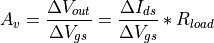
This equation, however, assumes very small AC input voltage, so that the output voltage change is still small.
So if we make the small signal voltage gain 100, and we set the AC input voltage amplitude to 1mV, then the AC output voltage amplitude will be 100 * 1mV = 0.1V.
10.4.2. Output Voltage Swing - Maximizing It with Bias Point Design
Now if , is not going to have an amplitude of 2V * 100 = 200V. Rather will saturate as we have demonstrated with a real amplifier.
When is below threshold, the transistor cuts off. Thus, the highest possible is .
When is very high, the current will increase, and hence pull down .
For an ideal transistor with an ideal knee voltage or with a drain saturation voltage , the best low we can achieve occurs when , and decreases to zero.
If we further assume that the transistor is linear, we find that a maximum output voltage swing of / 2 can be obtained if we choose a DC equal to , as shown in figure 2.
Well, real MOSFETs are not so ideal, as we have seen from measured curves. The relation is not exactly linear but not too far off, either. The knee voltage, or , at which saturation occurs can be quite a bit above 0V, however. That fact can be taken into account by setting aside voltage room for the transistor to saturate. The consequence is basically that the lowest will not be zero volts.
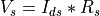
10.4.3. Stabilizing DC Bias Point with a Resistor at Source
We have seen that the output voltage and current swing have a lot to do with the DC and DC , which we denote as and . Together they are called the DC bias point.
It is necessary to stabilize the DC bias point against fluctuations of , temperature, K factor, or even transistor threshold voltage.
Take an increase in for example. It directly translates into a increase, which then increases .
With a resistor between source and ground, as shown in figure 3, an increase of increases , which then increases .
Figure 3: MOSFET amplifier with feedback resistor.
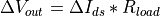
The increase, however, increases . Consequently, the resulting increase is less than the original increase from the increase, simply because .
The resistor is thus said to act as a negative feedback, as it negatively affects the increase of .
For an AC signal, we do not necessarily want the large negative feedback.
Assume we want all of the AC input voltage to appear across , without any drop over . We can just add a large enough capacitor across , so that is shorted out by the capacitor, as shown in figure 3.
Choose a reasonable for stability of dc bias, this sets .
Find necessary to produce the given.
In simulation, just connect the drain and gate together for saturation operation, force a current of , and read the voltage value.
In the lab you can run a 2-wire analyzer measurement in the same way that you found the threshold voltage from a given threshold current.
Find .
Find R1 and R2 that will give the desired .
Approximately set .
Determine .
We can consider the finite in design and simulation. For first order design, the above simplification works just fine, and greatly simplifies the design.
A larger means more feedback, and gives a more stable dc bias point against , temperature, transistor , and transistor K variation. However, more means less voltage room to work with. Remember that is the available voltage room to work with. Furthermore, for real transistors, we have to choose to be approximately above to be in the saturation region.
R1//R2 (R1 in parallel with R2) will be the input impedance seen by the ac voltage source (shown in figure 4).
Figure 4: MOSFET amplifier with feedback resistor and DC blocking capacitors.
Normally we want R1 // R2 to be large, say around 100 or more.
Generally, we do not want R1//R2 to be small, as it will place too much of a load on the AC source. A small means a large input current requirement, or a “heavy” load. An extreme example would be a short circuit of a load to a source.
Normally, when we think of an AC signal, it is centered about zero volts. Think about the signal driving your speakers. However, if the output of the amplifier is taken directly from the drain, it will have a considerable DC bias. The solution is the addition of a capacitor at the output, as shown in figure 4. This capacitor will allow the amplified signal to pass, but not the DC bias. That is why they are called DC blocking capacitors, or alternatively, AC coupling capacitors.
A capacitor is also needed at the input. Otherwise, the gate voltage might be changed by the device that is driving it. Worse, the device connected to the amplifier might be damaged by the gate voltage. Think about connecting the line out jack of a CD player to a stereo.
We can immediately recognize the 4R biasing circuit used.
Note that we have two Re’s,
Re1 and Re2, Re1 is for negative feedback in “ac” signal.
Re2 is for negative feedback in DC bias.
Exactly how to choose (, )
will take more discussions which will be
covered in Analog Electronics.
For now, let us consider that we have been given a (, ) bias point.
We have designed a biasing circuit to produce the required (, ) using
a Si bipolar transistor, 2N3904 in this experiment.
We have added 3 capacitors that are going to block DC
and pass AC. Of course, each capacitor’s
impedance depends on frequency.
A photo of a bipolar transistor amplifier using 4R bias is shown below in
figure 6.
Figure 6: Bipolar transistor amplifier on ELVIS breadboard.
Find the gate-source voltage necessary for a 1mA drain current. You may find this multisim file helpful: download. It contains the correct model for the MOSFET used in the lab.
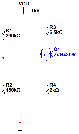
Design a 4 resistor biasing network for a MOSFET with a drain current of 1mA, 2v source voltage, and an input equivalent resistance of 110 . The input resistance is defined as R1||R2. is 15v. A sample circuit is shown in figure 7.
Verify the DC operating point of your bias network with Multisim. Measure , , and . Use the ELEC2210_ZVN4306A (used in prelab step 1) as the MOSFET.
Add 1 F capacitors to your circuit, as shown in figure 8, and then simulate your amplifier using Multisim. Select AC Analysis and sweep from 10Hz to 5MHz. Plot Output/Input.
In order to make your graph show up better when printed (and save toner), use a white background. From the grapher view menu bar select Graph > Black and White Colors.
Construct a biasing network for a ZVN4306 using the resistor values calculated in the prelab. Use +15v for . If the exact value is not available, use the next closest resistor.
Connect the function generator to the input of the amplifier. Select a 5kHz sine wave, .05vpp.
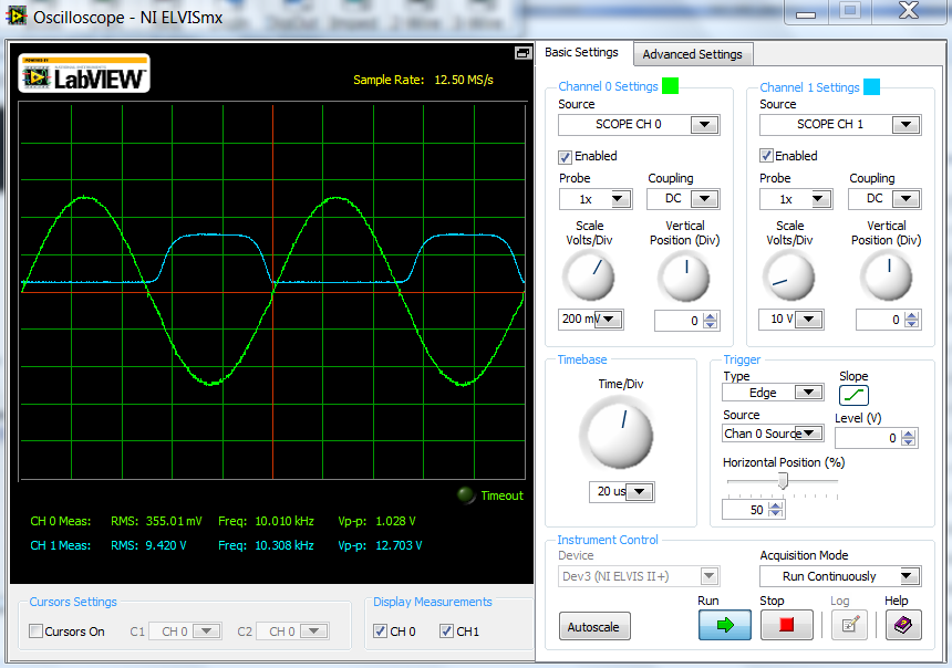
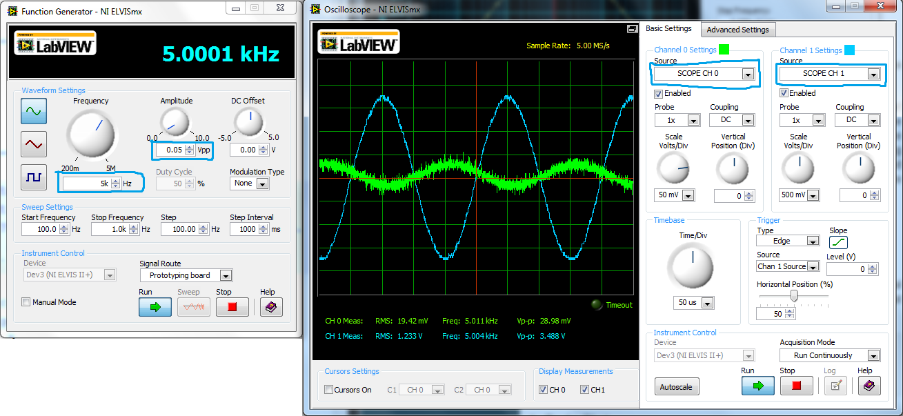
Connect the input of the amplifier to scope CH0 and connect the output to scope CH1. Be sure to select SCOPE CH0 and SCOPE CH1 on the oscilloscope SFP, as shown in figure 9. Because we will need to take measurements at frequencies higher than the analog inputs’ sampling frequency, they cannot be used. The BNC jacks and analog inputs should already be tied together on your board, so that either will work. Otherwise, be sure to use the BNC jacks on the side of the ELVIS base.
Take screenshots of the output and input waveforms at
several frequencies: 500Hz, 5kHz, 50kHz for calculating
ac voltage gain later in lab report.
Use the formula Gain = . Only absolute value is required, but you should
notice that transistor is naturally inverting in this amplifier configuration.
Select a scale large enough that allows accurate amplitude measurements.
Make measurements and take screenshots so that you can
later calculate the ac voltage gain’s absolute value
for the following input amplitudes at 5kHz: .1vpp, .4vpp, .7vpp, 1vpp, 1.3vpp.
Note
Keep in mind that as you adjust the input amplitude,
your scope settings will need to be adjusted accordingly.
The entire waveform must be visible on the scope display
in order to make accurate measurements.
Using the second scope channel, measure the drain and source voltages for an input of 5kHz, 1.3vpp. See figure 10 below for an example of the drain voltage.
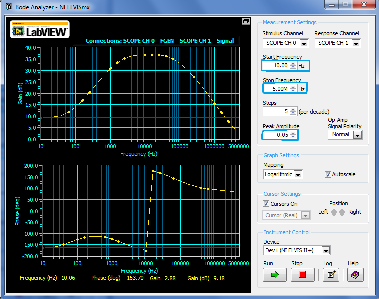
Open the Bode Analyzer. Set the start frequency to 10Hz and set the Stop frequency to 5MHz. Use a peak amplitude of .05, as shown in figure 12. Take a screenshot.
Disconnect the function generator from the input of your amplifier. Leave CH0 connected to the function generator.
Take two pieces of wire about a foot long. Connect one wire to the FGEN terminal and connect the other wire to the input of your amplifier. Both wires should be vertical and parallel to one another, but not touching.
Set the function generator to produce a 300 kHz, 10vpp sine wave.
Observe the transmitted and received waveforms on the scope. Take a screenshot
Construct the BJT amplifier shown below in figure 13. Notice that the circuit is exactly like the MOS amplifier with the exception that the MOS transistor is replaced by a BJT 2N3904.
Set the function generator to produce a 10kHz, 0.01Vpp sine wave.
Measure the input and output of the amplifier using the scope. As we do not have AC negative feedback, the voltage gain is high.
Use the dynamic signal analyzer to measure the output spectrum for a 5kHz .05vpp sine wave input. Be sure to set the source to CH1. Take a screenshot of the output signal spectrum, similar to the one in figure 11.
Open the Bode Analyzer. Set the start frequency to 10Hz and set the Stop frequency to 5MHz. Use a peak amplitude of .05, as shown in figure 12. Take a screenshot.
 resistor
 F capacitor
 resistor
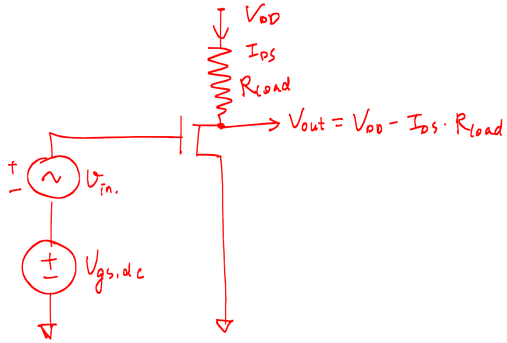
 .
.
 is called the transconductance gm.
 ,
,  is not going to have an amplitude of 2V * 100 = 200V. Rather
  will saturate as we have demonstrated with a real amplifier.
 is below threshold, the transistor cuts off. Thus, the highest
  .
. .
. , the best
  , and
, and  is linear, we find that a maximum output voltage swing of
  / 2 can be obtained if we choose a DC
  equal to
  , as shown in figure 2.
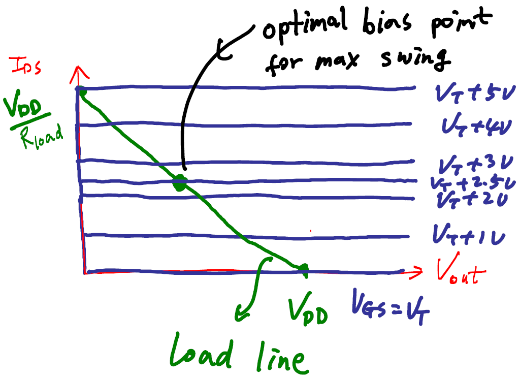
 is simply the ratio of the voltage swing (
 or
or  ) to current swing (
 ):
):
 curves. The
  , at which saturation occurs can be quite a bit above 0V, however. That fact can be taken into account by setting aside voltage room for the transistor to saturate. The consequence is basically that the lowest
  and DC
  increase, which then increases
  , which then increases
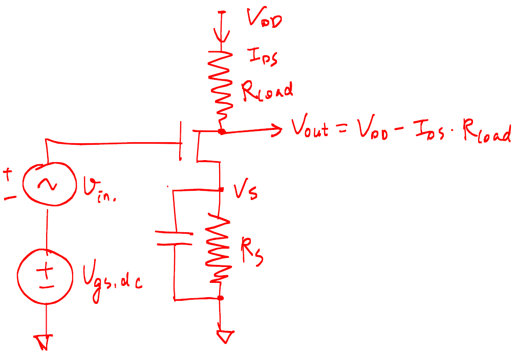
 . Consequently, the resulting
  .
. resistor is thus said to act as a negative feedback, as it negatively affects the increase of
  for stability of dc bias, this sets
  .
. .
. .
. .
. .
. , and transistor K variation. However, more
  is the available voltage room to work with. Furthermore, for real transistors, we have to choose
  to be in the saturation region.
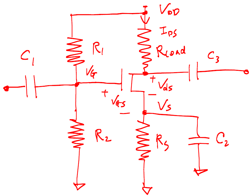
 means a large input current requirement, or a “heavy” load. An extreme example would be a short circuit of a load to a source.
 ,
,  )
will take more discussions which will be
covered in Analog Electronics.
For now, let us consider that we have been given a (
)
will take more discussions which will be
covered in Analog Electronics.
For now, let us consider that we have been given a (
 ,
, 
 . Only absolute value is required, but you should
notice that transistor is naturally inverting in this amplifier configuration.
Select a scale large enough that allows accurate amplitude measurements.
. Only absolute value is required, but you should
notice that transistor is naturally inverting in this amplifier configuration.
Select a scale large enough that allows accurate amplitude measurements.