This experiment is designed to introduce real world characteristics of bipolar junction transistors (BJT) and a few of their applications. Specifically,
We will measure forced base current and forced base-emitter voltage IC-VCE characteristics
We will construct a bipolar transistor inverter circuit to better understand the concepts of voltage and current saturation
We will learn how to use a bipolar transistor to turn on a large current with a small voltage or current
We will learn how to make voltage transfer curve (VTC) measurements, which is an important technique for designing a wide variaty of analog and digital circuits, including amplifiers and logic gates
We will gain more experience with the ELVIS II+ breadboarding system
We will continue to develop professional lab skills and written communication skills
A thorough treatment of BJTs can be found in Chapter 5 of the ELEC 2210 textbook, Microelectronics Circuit Design by R.C. Jaeger.
The acronym BJT stands for Bipolar Junction Transistor.
BJTs can be viewed as a device that controls an output current,
the collector current typically, with either an input current or voltage.
The experiments here are designed to help you understand fundamental
transistor current-voltage (I-V) characteristics in the real world,
as well as key concepts behind the use of a bipolar transistor in amplifiers and switches.
We will use 2N3904, a general purpose npn BJT with a maximum working current of 200 mA and a maximum power dissipation of 625 mW.
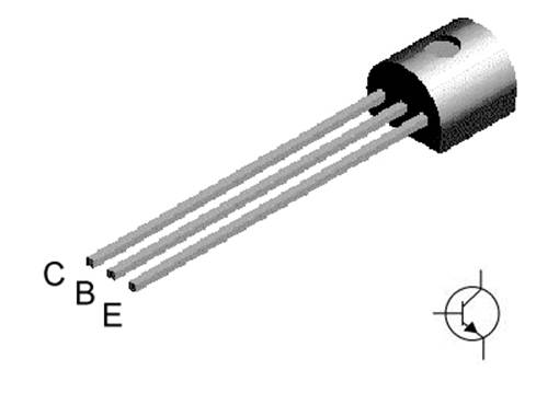
The C, B, and E terminals can be identified in figure 1.
For each curve, the forward active region is the region to the right of the knee, i.e., the nearly flat part. The region to the left of the knee is the saturation region. For switching applications, the BJT is most like a closed switch when it is in the saturation region, where VCE is small. It is most like an open switch when it is in cutoff, with iC = 0.
A BJT is often used as a current-controlled switch, as illustrated in figure 3.
For most switching applications, the BJT is operated in the saturation region when it is conducting current. In this region, the voltage drop across the BJT collector-emitter terminals is small, as desired. The amount of load current in this case is determined by the value of VCC and the load characteristics, and is essentially independent of input current or the BJT characteristics.
Obtain the data sheet for the 2N3904 here, and use it to find the range of forward current gain (Fo, also known as hFE). Learn how to tell apart the emitter, base, and collector. Draw a 2N3904 with the terminals labeled.
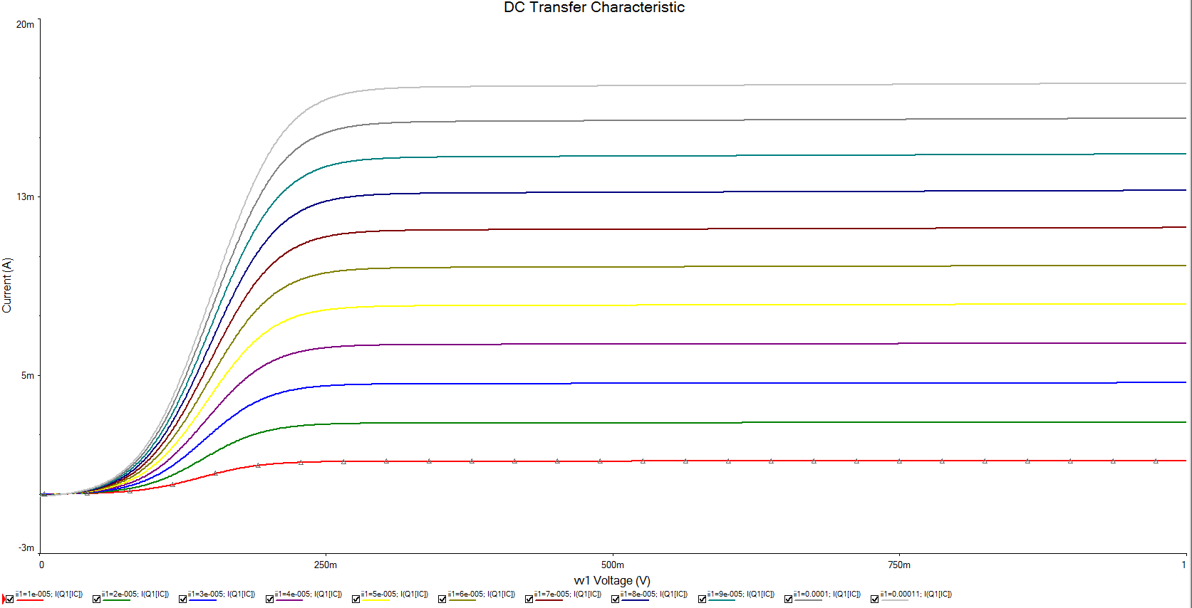
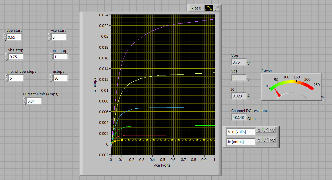
Simulate the circuit shown below in Multisim. Select DC Sweep as the type of analysis. Source 1 is the voltage source. Sweep from 0 volts to 1 volt in .001 volt increments. Check the box labeled “Use source 2” to do a secondary sweep. Source 2 is the current source. Sweep from 0 amps to .00001 amps in .000001 amp increments. The output is the collector current. It is the variable called I(Q1[IC]).
The output characteristics of a similar circuit are shown below in figure 5.
Figure 5: Simulated output characteristics of a 2N3904.
In which region should the BJT be operating when it is a “closed switch?” Why? In which region should it be operating when it is an “open switch?” Why?
Open the 3-wire current voltage analyzer soft front panel.
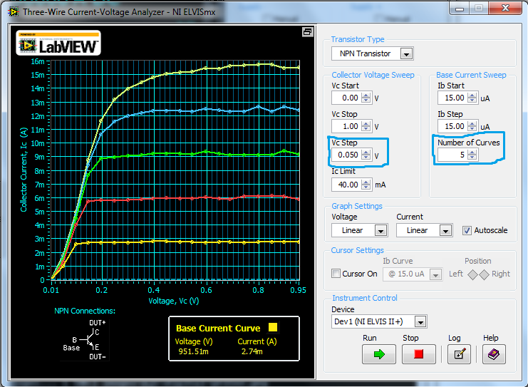
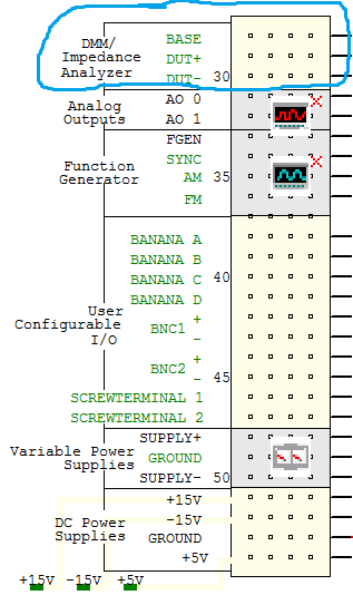
Carefully measure the forced IB output characteristics of the 2N3904 NPN transistor as follows. Set the Vc step to .05 volts and set number of curves to 5 as shown in figure 7. Connect the collector to the DUT+ terminal (pin 29 on the lower left terminal strip), connect the emitter to the DUT- terminal, and connect the base to the BASE terminal shown in figure 7. When looking at the flat side of the transistor, the leads are emitter, base, and collector from left to right, as shown above in figure 1.
Click run. The curve tracer should slowly draw the plot.
Click log to save the data for later analysis. Save a screen shot also. Using Excel or Matlab, plot as a function of VCE for IB = 30 uA. Identify the saturation region and forward active regions from your screenshot.
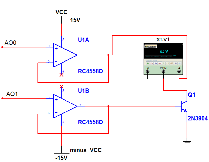
We will now measure how IC changes with VCE for forced base-emitter voltages. The analog outputs will be used to set the base and collector voltages, while the collector current is measured with the ELVIS multimeter. Because the analog outputs have a very small current capacity, two non-inverting unity gain op-amps will be used.
Build the circuit shown in figure 9. Only one RC4558 op-amp is required; there are two amplifiers on each chip. Connect the non-inverting inputs to the ELVIS analog outputs (pins 31 and 32) as shown.
Figure 9: Schematic for measuring forced Vbe characteristics.
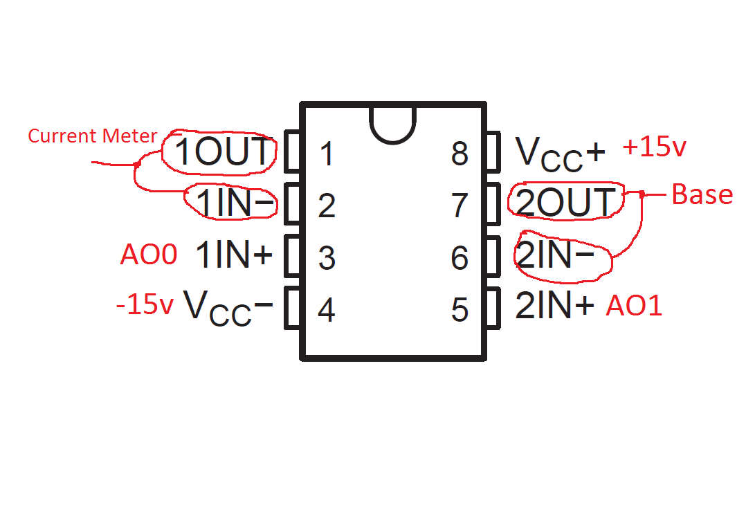
Figure 10 shows the outline of a 4558 op-amp with the pins labeled.
A widely used technique in understanding circuit operation is to sweep an input or source voltage,
and observe how an output voltage of interest responds.
In circuit simulation, this is done using a DC voltage sweep
analysis. The result is a voltage transfer curve (VTC).
VTCs are useful in analyzing a wide range of analog and digital circuits.
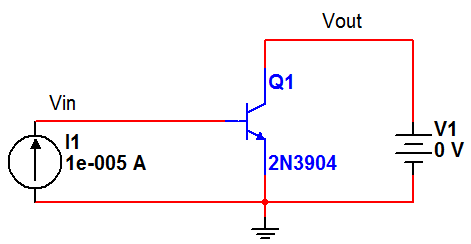
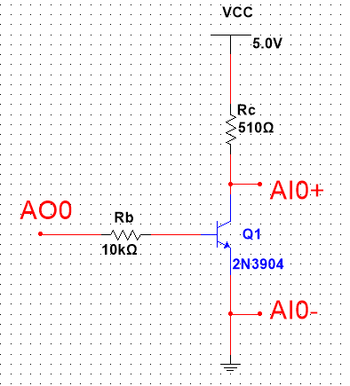
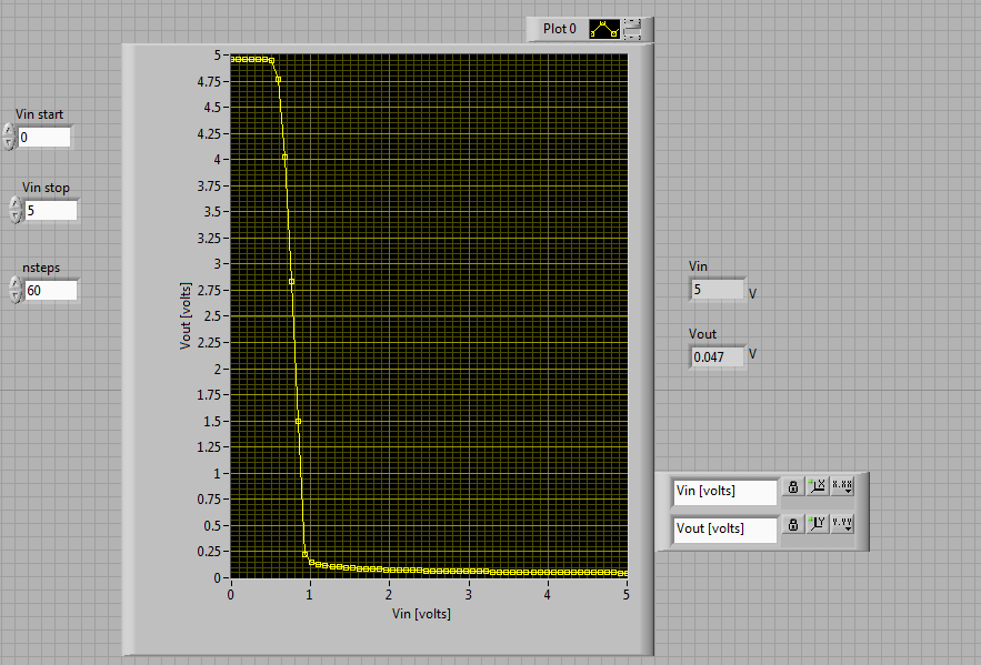
Here we will use the analog output AO0 to provide a programmable input voltage,
and use AI0 to experimentally measure the output voltage of a NPN transistor switching circuit.
The circuit here is essentially a BJT inverter, which can also be used as an amplifier
when bias point is set to the region where the output voltage changes fastest with the input voltage.
Construct the circuit shown in figure 12. The +5V terminal is the bottom pin on the lower left terminal strip.
Reconnect AI0+ and AI0- across the collector load resistor. Re-run the program. Save a screenshot. Right click on the graph and export the data for later analysis.
Reconnect AI0+ and AI0- across the resistor in series with the base. Re-run the program, and save a screenshot. This data can be used later to calculate the base current.
Reconnect AI0+ and AI0- across the base and emitter. Re-run the program, and save a screenshot.
You can modify the sweep step if needed.
What to do in your lab report?
Discuss, at what Vin the output voltage starts to drop appreciably? How does this compare to 0.7V, the turn on voltage of a Si PN junction? Recall that the base-emitter junction is essentially a PN junction, only the electron current gets transported to the collector.
Identify the 3 distinct regions of operation (cutoff, forward active, reverse active or saturation) on the Vout-Vin curve.
Plot IC and IB versus Vin. Explain how beta, the ratio of IC/IB, changes with Vin.
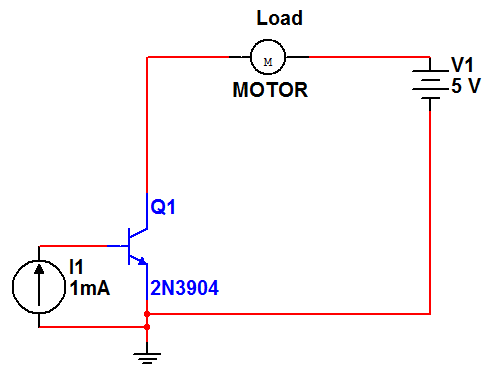
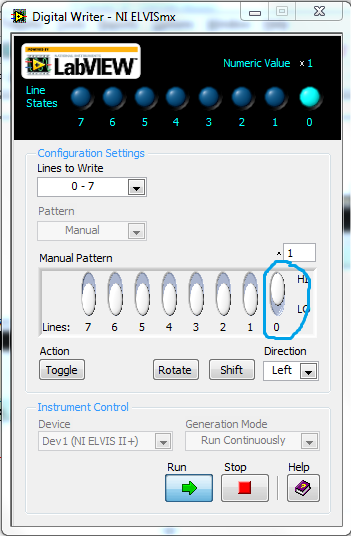
Here we use the transistor as a switch to turn on and off a load, which can be an LED, a fan or a speaker. A low input voltage or current turns the collector current off. A high input voltage or base current turns the transistor on. The natural current amplifying ability of the transistor allows us to switch on and off a much larger current using a source that has limited current drive capability, e.g. the output of a digital chip. We will mimic the output of a digital chip here with the digital writer.
Transistors can be used as switches when we want to connect a load to an integrated circuit that the ic cannot drive. Here the transistor is used as an electronic relay. Another way to think of it is that the transistor is used to amplify the chip’s limited current output to power a much larger load. In this lab, a NPN transistor will be used to drive a fan. The transistor itself will be controlled by the ELVIS digital writer, which would not normally be able to power a fan.
Construct the circuit shown in figure 14. The digital I/O pins are on the top right terminal strip. Use DIO 0 (pin 1). To use the multimeter to measure current, the COM and A jacks must be used, not the V ->|- jack as used earlier. Also note that the ammeter must be connected in series with the circuit.
Figure 14: Circuit connections for demonstrating BJT as a switch.
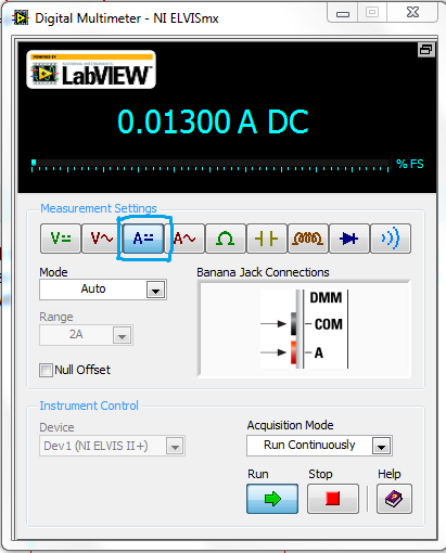
Open the Digital Multimeter, select DC Current, and click run as shown in figure 15.
Measure and record in a table the values of VCE, VBE, VBC, IB and IC when the LED is on and when it is off. In order to determine IB, measure the voltage drop across RB using either the Fluke DMM or the ELVIS DMM, and use Ohm’s law to calculate the base current. If the onboard voltmeter is used it will be necessary to disconnect the current meter from the collector.
Can you confirm that the BJT is in saturation when the LED is on, and in cutoff when the LED is off? (Hint: In saturation, both junctions should be forward biased. In cutoff, both junctions should be reverse biased.)
Replace Rb with a 1 resistor. Replace the LED and 330 ohm resistor with a fan and repeat.
Observe the fan polarity (black wire should be connected to the collector of the BJT, red to the DMM).
Measure and record VCE, VBE, VBC, IB and IC when the fan is on and when it is off. Does the transistor still saturate when the fan is on?
 Fo = 25 and VA = 8 are shown in figure 2.
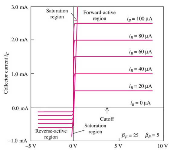
 ->|- jack as used earlier. Also note that the ammeter must be connected in series with the circuit.
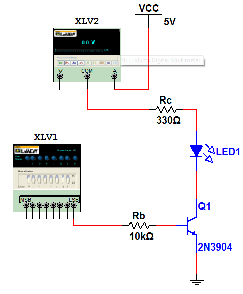
 resistor. Replace the LED and 330 ohm resistor with a fan and repeat.
Observe the fan polarity (black wire should be connected to the collector of the BJT, red to the DMM).
Measure and record VCE, VBE, VBC, IB and IC when the fan is on and when it is off. Does the transistor still saturate when the fan is on?
resistor. Replace the LED and 330 ohm resistor with a fan and repeat.
Observe the fan polarity (black wire should be connected to the collector of the BJT, red to the DMM).
Measure and record VCE, VBE, VBC, IB and IC when the fan is on and when it is off. Does the transistor still saturate when the fan is on?