This starts Part II of our lab experiments which are
directly related to the lecture material of Elec 2210.
Again, it is mandatory for you to read the lab manual and complete the pre lab assignments.
There will be “What to do in lab report” sections in the lab procedures.
Observe those requirements
so that you take necessary measurements needed for reporting.
The experiments in this laboratory exercise will provide an introduction to diodes. You will use the ELVIS II+ breadboarding system to build and test several DC and AC diode circuits. The objectives of this experiment include:
Review basic principles of diodes from ELEC 2210
An understanding of diode rectifier circuits
More experience with the ELVIS II+ breadboarding system and the oscilloscope
Continue to develop professional lab skills and written communication skills.
Diodes are circuit elements that allow current to pass in one direction, while blocking it in the other direction. They are used in rectifier circuits, which convert AC to DC, and in voltage regulation and voltage limiting circuits.
An ideal diode has the following Shockley I-V characteristics:
At 300K, mV, the voltage difference
corresponding to 10x current difference is 60 mV
theoretically for ideal diodes.
Higher order physical
effects degrade the I-V slope. As a result, it takes more
than 60 mV voltage increase to
increase the current by one decade, or 10x.
From (1), we can see that the diode current increases exponentially as the diode voltage becomes more positive (forward bias), but the current is asymptotically limited to -IS when vD is negative (reverse bias). If the diode is forward biased substantially, Equation 1 can be simplified to a pure exponential, and then near room temperature we can deduce the 60 mV per decade rule, which says that Vf increases approximately 60 mV for every factor of 10 increase in Id.
In addition to the behavior described by (1), all diodes have a reverse breakdown voltage, VBR, at which significant reverse current will begin to flow. For many applications, it is desirable to have VBR be as large as possible. For other applications, such as voltage regulation, we require relatively low reverse breakdown voltages, such as 5 V or 9 V. For these applications, we use Zener diodes. The reverse characteristics of a typical Zener diode measured using ELVIS are shown in Figure 1.
Figure 1: Current-voltage characteristics of a typical zener diode.
Real diodes have series resistance and junction capacitance which affect their behavior in circuits at higher currents and higher frequencies. Furthermore, IS is a strong function of temperature. These effects will not be considered in this lab experiment.
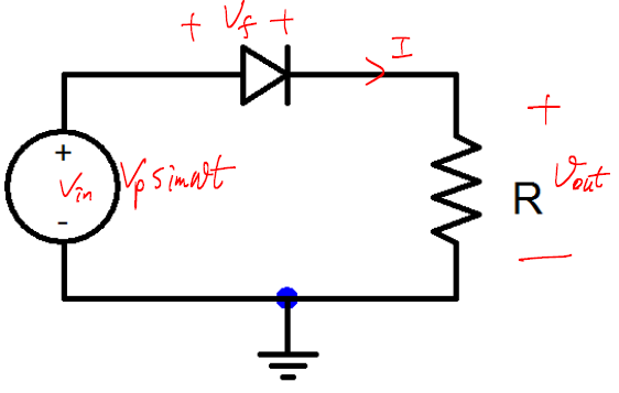
Vout = I*R. When Vin is greater than zero, I is greater than zero and Vout is greater than zero. When Vin is less than zero, both I and Vout are approximately zero.
Current will flow in only the forward direction through the diode, as long as the peak negative value of the voltage does not exceed the reverse breakdown voltage of the diode. In this case, Vout will never be negative, thus the AC voltage is said to be rectified. The resulting waveform will be only the top half of the input sine wave.
However, to create what would be considered direct current, we will also need a capacitor. The filter capacitor is placed in parallel with the load resistance in a power supply. Its purpose is to filter out the voltage fluctuations in the rectified waveform.
On most diodes, the p-type terminal is marked with a red band and the n-type terminal is colored black. The red end is called the anode and the black end is called the cathode. It is easiest to remember that current flows from the positive to the negative terminal, or from red to black. Because LEDs are often clear, a different system is used. The long lead of an LED is a the positive one. This system is also used to identify the polarity of other components. For example, the longest lead of a polarized capacitor is also positive.
As we saw in the previous section, diode is a useful component to design rectifier circuits that convert alternating (or bipolar) signal into unipolar signal, that can then be filtered to obtain a constant level. Here we present design equations for the half-wave and full-wave bridge rectifier that you will build in the lab. For a half-wave rectifier, that has a sinusoidal input of period , peak voltage of , and diode-on voltage , then the peak-to-peak ripple voltage is given by –
where is the load resistance and is the capacitance of capacitor connected in parallel with the load resistance.
For a full-wave rectifier, the peak-to-peak ripple voltage for the same sinusoidal input is smaller (why?) than the half-wave rectifier and is given by –
Using the ripple voltage , we can also find the conduction time interval, , which is basically the time duration for which any diode conducts in each period, for both the half-wave and full-wave rectifier using the following result:
Peak inverse voltage, PIV, is defined as the maximum reverse voltage sustained by any diode during each period. PIV for half-wave rectifier is given by , while for a full-wave (bridge) rectifier it is given by .
Using the formulas from Equations (4), (5), and (6) [not the equations given in our class notes or text], calculate the ripple voltage,
conduction time interval,
and peak inverse voltage
for both a half-wave rectifier
and a full-wave (bridge) rectifier
with the following parameters: 100Hz, 10 volt peak-to-peak input, 20k load resistance, 1 F filter capacitor, 0.6 volt diode turn on voltage.
Note
The equations for ripple voltage developed in our lecture notes and text assume
a very small ripple voltage, and near DC output. This can
result in large errors, as you will find out when comparing
hand calculation with simplified equations with simulation and measurement. So you are better off using the more accurate equations given for half-wave [Equations (4) and (6)] and full-wave rectifiers [Equations (5) and (6)].
Simulate the same two circuits in multisim using 1N914 diodes.
Find the ripple voltage, conduction time interval, and peak inverse voltage.
Take screenshots for prelab report. Compare the results of your simulations with your calculated values.
A sample file is provided for each circuit, however the parameters must be changed. Note that the sample file contains two circuits. Either can be used. However, one of the circuits is connected to simulated versions of the instruments used throughout the rest of the lab.
You need to change your scope channel input connections to measure
a different voltage. In simulation, you can also use more scopes
to display more voltages, as you see in the full wave sample file.
You can also use the grapher and type in an expression to observe a different
voltage, e.g. the reverse voltage across a particular diode.
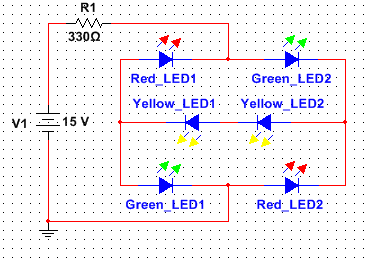
One use of diodes is to prevent damage to components when power supply polarity is reversed. For example, consider the circuit shown in Figure 3. When the power supply is connected normally, both the green and yellow LEDs light up, indicating that current is flowing through them. However, when the power supply polarity is reversed, the red LEDs will turn on. In both cases, the yellow LEDs will illuminate.
Construct the circuit shown in Figure 3. In order to make the circuit easier to understand, use the pin holes instead of wires to connect the red and green LEDs to one another.
Swap the +15v and ground wires.
What to do in lab report
Explain why the red and green LEDS never light up simultaneously.
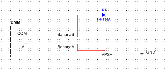
4.6.2. Diode I-V characteristics with Custom LabVIEW Program.
Make circuit connections as shown in Figure 4. VPS+ is the positive variable power supply.
Figure 4: Zener diode schematic with connections on ELVIS for forward IV characteristics.
Turn on both the ELVIS base and the power to the breadboard.
Download the LabVIEW program here for plotting forward IV characteristics of the 1N4733 diode.
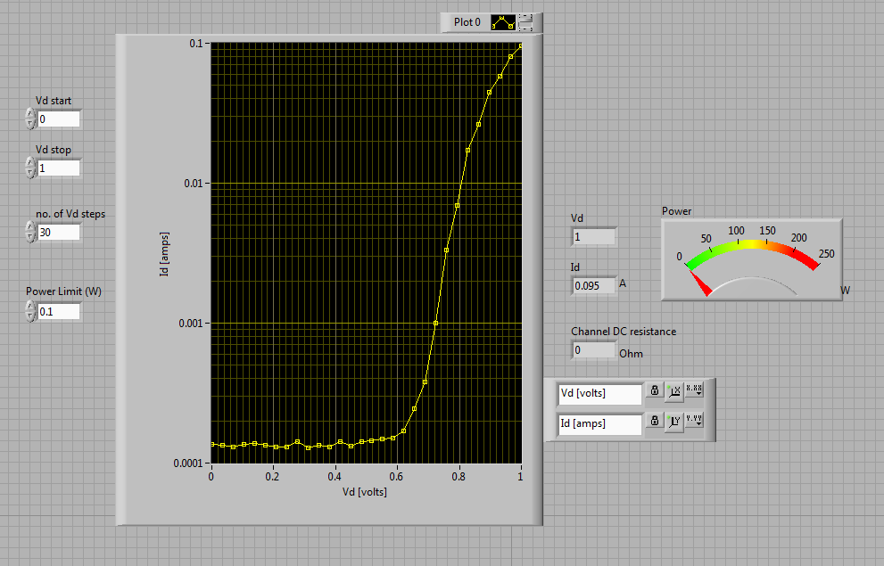
Set the Vd start voltage to 0V, and Vd stop to 1V. Set number of steps as 30. Click run. Right click on the plot to save the measured data for use in lab report. Take a screen shot. You should see a plot like one shown in Figure 5.
Figure 5: Zener diode forward IV characteristics, with Vd start and stop settings.
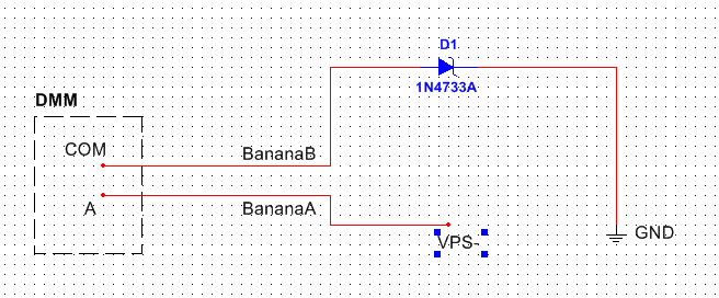
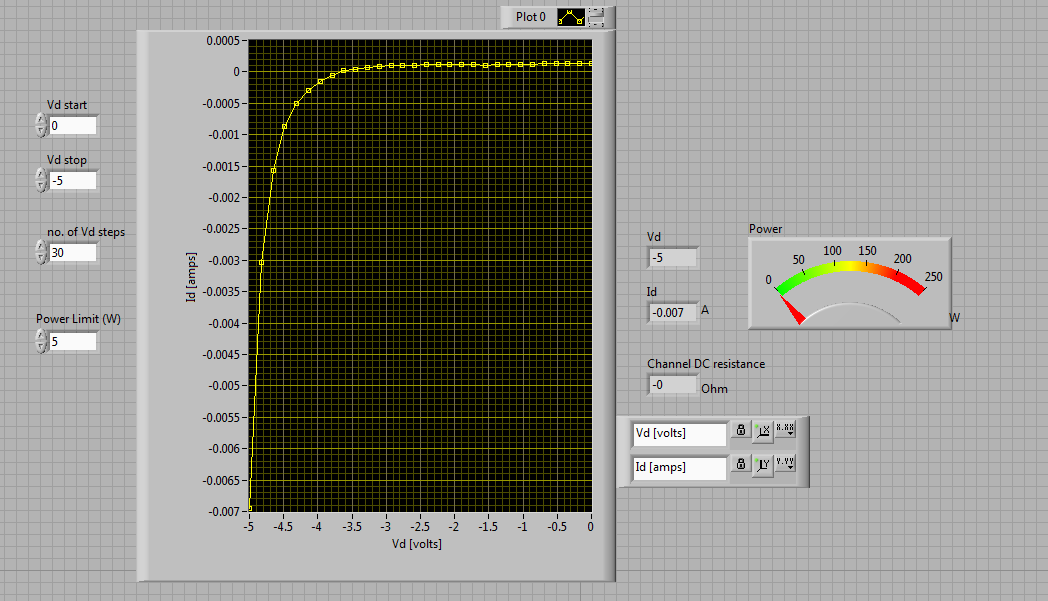
We shall now plot the reverse characteristics of the zener diode. First turn off power to the breadboard. Make the connections as shown in Figure 6. It just entails swapping VPS+ with VPS- in the earlier circuit.
Figure 6: Zener diode schematic with connections on ELVIS for reverse IV characteristics.
Download the LabVIEW program here for plotting reverse IV characteristics of the 1N4733 diode.
Set the Vd start voltage to 0V, and Vd stop to -5V. Set number of steps as 30. Click run. Right click on the plot to save the measured data for use in lab report. Take a screen shot. You should see a plot like one shown in Figure 7.
Figure 7: Zener diode reverse IV characteristics, with Vd start and stop settings.
What would you estimate is the reverse breakdown voltage of the zener diode? Does breakdown occur abruptly?
What to do in lab report
Show all screen shots.
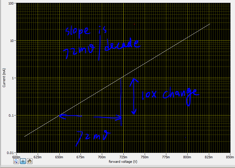
Using the data file saved above, estimate the voltage difference between two points of 10x current difference in the linear region when the current axis uses log scale.
Compare your result with the 60 mV per decade rule.
For example, use approximate current values of 5 mA, .5 mA or .6 mA, .06 mA to test the rule.
If you cannot find two current values in the linear region that are approximately a decade apart,
linear interpolation will be required.
Compare the corresponding voltage differences with 60 mV.
A graph made using data from this measurement is shown in Figure 8 and illustrates a 72 mV/decade slope. Note that a log scale is used for the current axis to facilitate observation of the voltage swing required for a 10x change of current.
Figure 8: How to find voltage difference required for 10x current change.
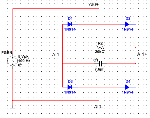
Construct the circuit shown below in Figure 9 using 1N914 diodes. To realize the 7.6 F capacitance, connect two 3.3 F and one 1 F capacitor together in parallel. 20k is a standard resistor.
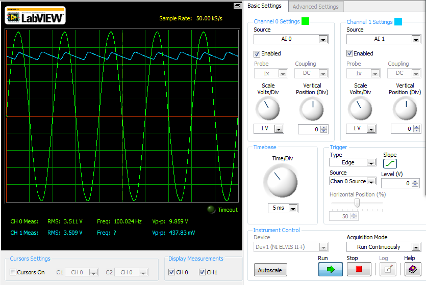
Set the function generator to 10 volts peak-to-peak to produce 5V peak. As the function generator is grounded, we must use a make a differential measurement of the voltage across the output. Make sure that the AI 1- terminal is not grounded. Instead connect the AI 1+ and AI 1- terminals to opposite sides of the resistor.
Save a screenshot of the capacitor voltage similar to the one in Figure 10.
Measure the ripple voltage and conduction time interval for comparison with prelab calculation and simulation.
Now remove one of the 3.3 F capacitors, resulting in a total capacitance of 4.3 F. How does the output change? Save a screenshot.
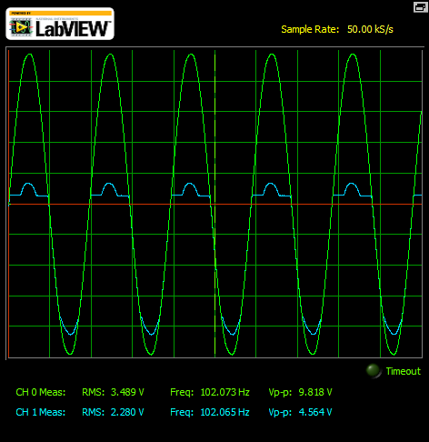
Now move the AI 1+ and AI 1- inputs to measure the voltage across D2.
Use the scope cursors to find the point when the inverse voltage across the diode D2 reaches its peak.
A screenshot of the voltage across D1 is shown in Figure 11.
Show all screen shots.
Is the measurement consistent with theory and simulation? During what time interval is D2 on?
Compare theory, simulation and measurement for R=20k , and C=7.6 F.
The previous diode based rectifier circuits suffer from
diode voltage loss. While this is no big deal for power adaptors, for low voltage rectifying applications,
this voltage loss can be too large.
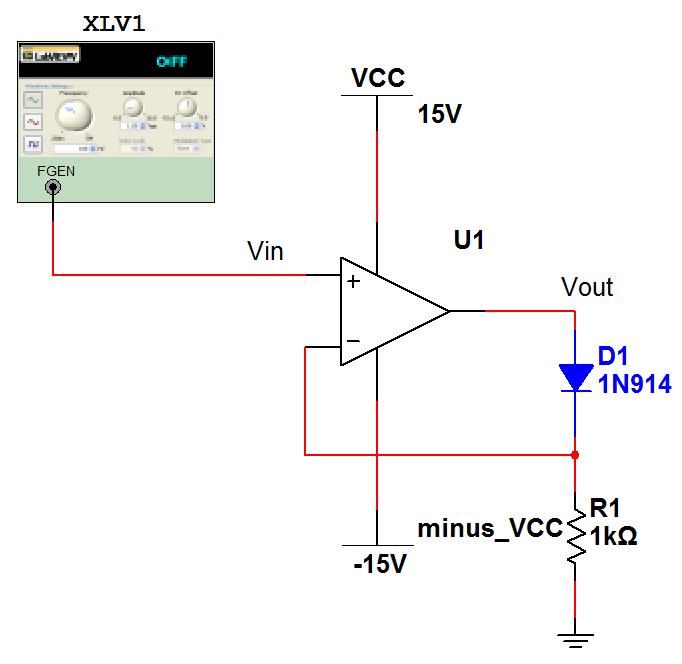
We can remove this diode voltage loss using a so-called super diode shown below.
Using the rc4558 op-amp available in the lab, construct the circuit shown in Figure 12.
You may not have used an op-amp before, that is okay. You need to supply power, actually two powers, one positive, and the other
negative. On the ELVIS, just use the +15V and -15V power supplies.
The rc4558 has two sets of inputs and outputs, or two channels. We will just use one set.
When Vin > 0, op-amp output Vout is positive, D1 turns on, allowing
a current to flow through R1. The impedances at the “+” and “-” inputs of the
op-amp are so high that their currents can be neglected for practical purposes.
The op-amp has high enough gain so that the + and - inputs
have about the same voltage levels.
This way, the output voltage of the rectifier
is the same as the input voltage during the positive half cycle.
When Vin < 0, Vout < 0, D1 turns off, the rectifier output is zero.
The combination of the op-amp and the diode configured in this
fashion is referred to as “super-diode.”
Measure the input and output of the rectifier with the scope.
This schematic did not indicate where to take the output.
It should be taken from the “-” input of the op-amp, which is connected to the load R.
Take a screenshot.
Add a capacitor to filter out the high frequency components.
What to do in lab report
Show one screen shot.
Describe an advantage of this circuit over the recitifer circuits built previously.
 resistor
![I = I_{s} [ \exp
\left(
\frac{V_{f}}{\phi_{t}}
\right) - 1 ],](_images/math/e2769bc98c1d379448f8d6fc65d97ab3fd1b50ad.png)
 = kT/q is the thermal voltage.
 and
and
 , the current ratio relates
to the voltage difference by:
, the current ratio relates
to the voltage difference by:
 mV, the voltage difference
corresponding to 10x current difference is 60 mV
theoretically for ideal diodes.
Higher order physical
effects degrade the I-V slope. As a result, it takes more
than 60 mV voltage increase to
increase the current by one decade, or 10x.
mV, the voltage difference
corresponding to 10x current difference is 60 mV
theoretically for ideal diodes.
Higher order physical
effects degrade the I-V slope. As a result, it takes more
than 60 mV voltage increase to
increase the current by one decade, or 10x.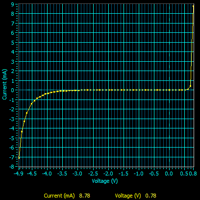
 , peak voltage of
  , and diode-on voltage
  , then the peak-to-peak ripple voltage
  is given by –
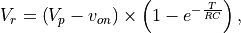
 is the load resistance and
  is the capacitance of capacitor connected in parallel with the load resistance.
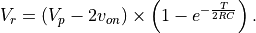
 , which is basically the time duration for which any diode conducts in each period, for both the half-wave and full-wave rectifier using the following result:
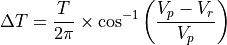
 , while for a full-wave (bridge) rectifier it is given by
 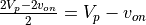 .
. load resistance, 1
  F filter capacitor, 0.6 volt diode turn on voltage.