Professor
-
EDUCATION:
- Ph.D., North Carolina State University, Materials Science and Engineering / Electrical Engineering (minor), 2001
- M.S., Yonsei University (Seoul, Korea), Materials Science and Engineering (Ceramic), 1995
- B.S., Yonsei University (Seoul, Korea), Materials Science and Engineering (Ceramic), 1993
-
EXPERIENCE AND EMPLOYMENT RECORD:
- 2013 to present : Alumni Professor, Materials Engineering, Auburn University
- 2018 to present: Director, Analytical Microscopy Center
- 2013 to present: Adjunct Professor, School of Advanced Materials Science & Engineering, Sungkyunkwan University
- 2013 to present : Professor, Materials Engineering, Auburn University
- 2008 to 2013 : Associate Professor, Materials Engineering, Auburn University
- 2003 to 2008 : Assistant Professor, Materials Engineering, Auburn University
- 2001 to 2003 : Postdoctoral Associate, Materials Science Division, Argonne National Laboratory
- 1997 to 2001 : Research Assistant, North Carolina State University
- 1995 to 1997 : Research Associate, Korea Institute of Science and Technology
- 1993 to 1995 : Research Assistant, Yonsei University (Seoul, Korea)
-
AWARD AND HONORS:
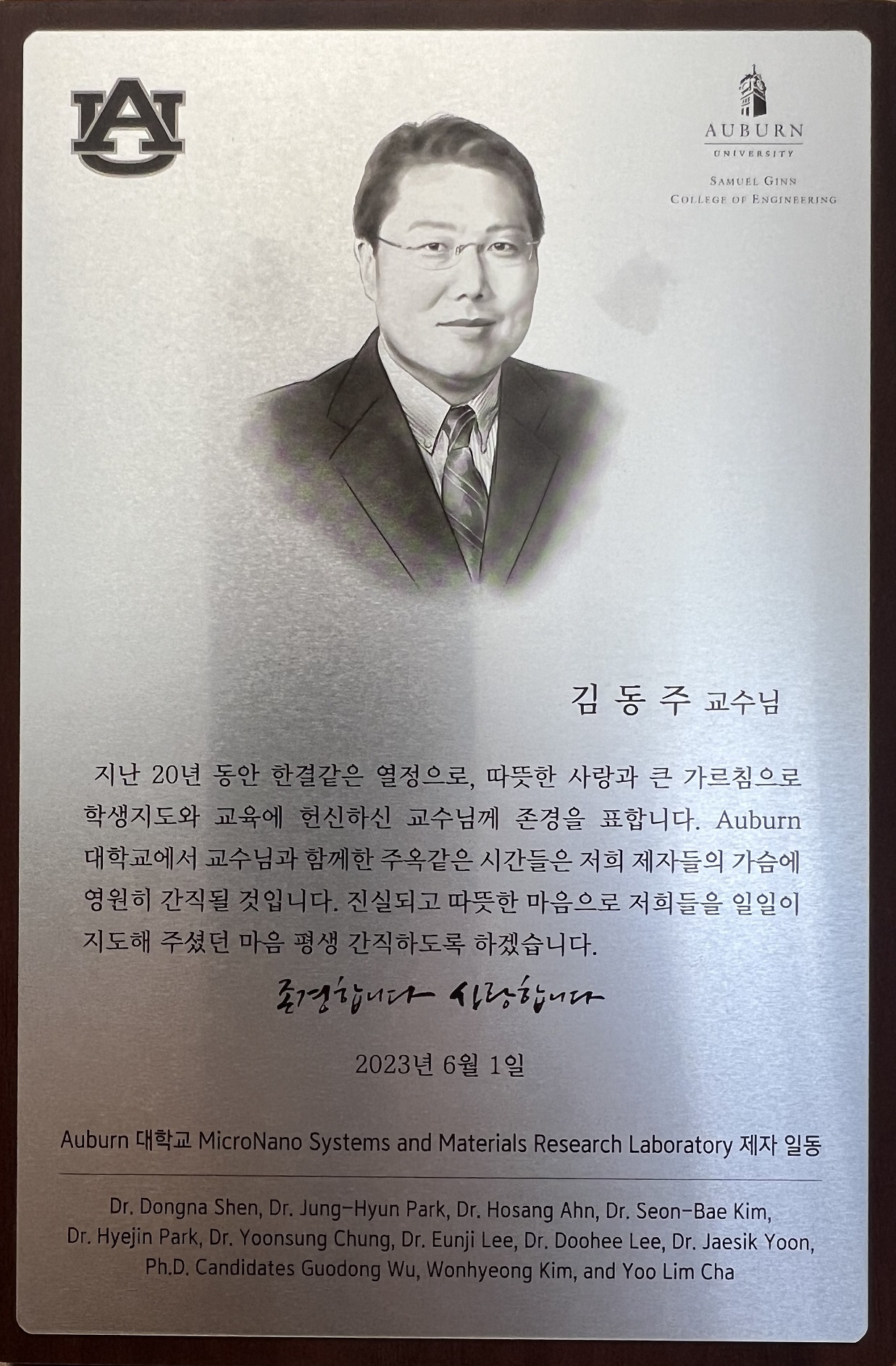
- AU SG College of Engineering, Outstanding Faculty Memeber (2023)
- Auburn University Alumni Professorship (2013-2018)
- AU Alumni Engineering Council Research Award for Excellence (2008)
- AWS Howard E. Adkins Memorial Instructor Award (2017-2018)
- AWS District Educator Award (2012), Meritorious Award (2010)
- Sigma Xi Honorary Society, Alpha Simgma Mu Honorary Society
-
PROFESSIONAL INVOLVEMENT:
- Executive Committee – ECS Sensor Division (2016 – present)
- Editorial Board Member: Nanomaterials, Materials, Physical B:Physics of Condensed Matter
- Chairman of AWS Auburn-Opelika Chapter (2009-2014)
- President of KSEA-Alabama Chapter (2010-2014)
- Members of ECS, MRS, IEEE, AWS, SPIE, SEM
- Journal Reviewer for ACS Sensors, Sensors and Actuators, Advanced Materials, Nature Communications, Journal of the Electrochemical Society, Journal of Micromechanics and Microengineering, Journal of Applied Phyiscs, etc.
- Proposal Review Panel Member for NSF, USDA, ACS, DOE, CRDF
-
EDUCATION INTEREST AND SUMMARY:
- Condition monitoring materials and systems: advanced sensing materials, energy conversion materials, flexible and wearable devices, portable energy conversion or storage devices
- Electrical ceramics : ferroelectric, dielectric, and piezoelectric ceramics for the majority of electronic applications
- Microelectronic materials and processing / Thin film science and technology : a fundamental understanding of basic science and present techniques with respect to solid state electronics, characterization of electronic materials, and thin film growth
-
SERVICE:
- Director – Analytical Microscopy Center, 2018 – present
- Member – SGCOE Curriculum Committee (MATL representative), 2015 – present
- Member – SGCOE Continous Improvement Committee (MATL representative), 2022 – present
- Member – University Senate, 2012 – 2015
- Chair – University Traffic and Parking Committee, 2011 – 2012
- Member – University Traffic and Parking Committee, 2009 – 2011; Member – Senate Library Committee, 2006 – 2009.
- Judge Committee - BEST High School and Middle School Robotics Competition (2004-2006)
April 2023
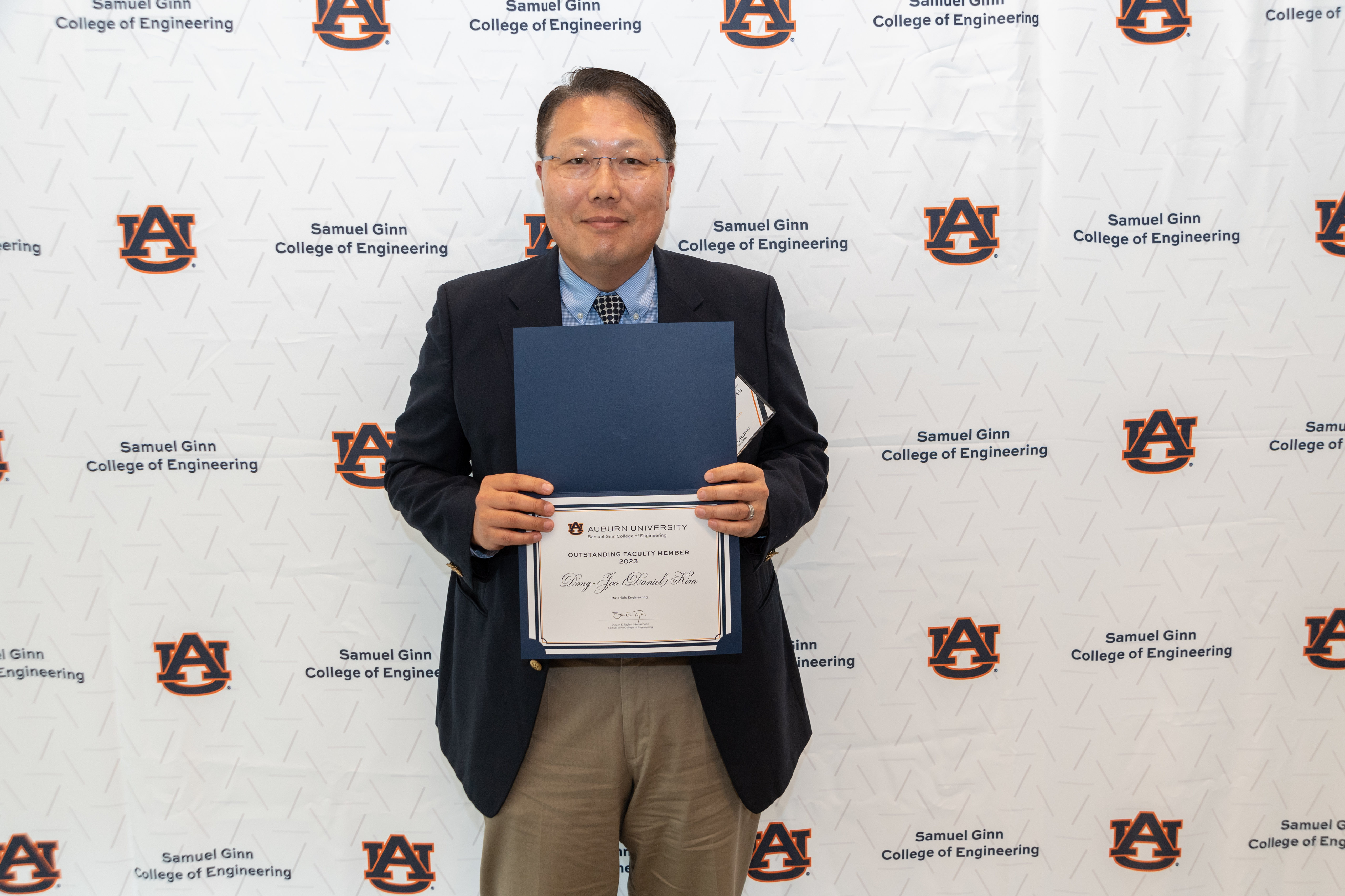
Outstanding Faculty Member of College of Engineering (2023)
Nov 2009
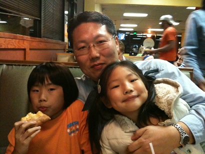
With my future scientists (?!).
Sep 2009
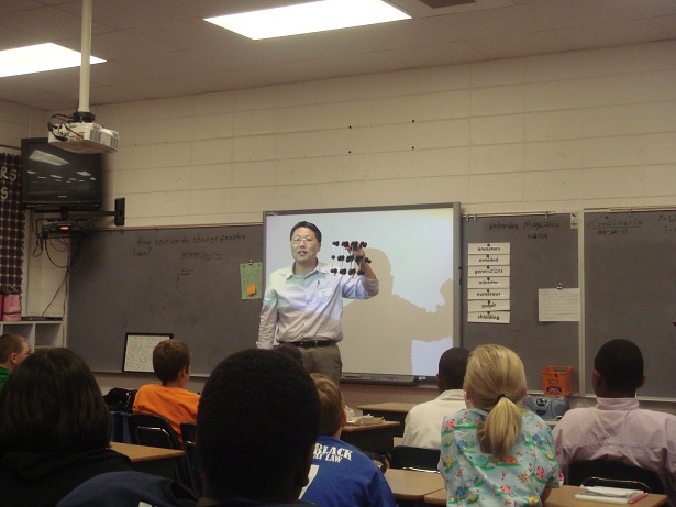
Outreach activity at local elementary school.