SiGe HBT - A Primer
A bite of history
World wide, SiGe HBT technology went through some very tough time before becoming a successful mainstream analog, RF and mixed-signal technology. At IBM, a world leader in SiGe technology, the history is a story of persistence (Dave Harame and Bernard Meyerson, IEEE TED, vol. 48, no. 11, p. 2555). The program began with an idea to replace a conventional implantation step, used in every silicon semiconductor bipolar process, by growing an in-situ doped alloy (SiGe), around 1987. A small group of people successfully persuaded a large digital computer manufacturer to invest in and eventually succeed in what was a new unproven technology for telecommunication applications in a field which IBM knew little about.
Commercial landscape
Today many companies have SiGe technology. The largest market for many years has been wireless transceivers (500MHz - 5GHz), some of which is now moving to RF CMOS, and many will continue to be in SiGe. SiGe also continues to find new applications.
0.35um and 180nm SiGe BiCMOS are most widely used for cellular, wifi, power management, and mixed-signal applications.
130nm is also available from all major foundries 90nm and 65nm SiGe BiCMOS exist but are not in mass production yet as we speak, but may well be soon when driver applications emerge, for instance, mm-Wave SoC, where pure CMOS is inadequate or no longer makes technological or economic sense.
Unlike in CMOS, where a new technology has a short lifespan of 2-3 years, a BiCMOS technology has a much longer (10 years roughly) lifespan.
SiGe advantages in a nut shell
SiGe has a smaller bandgap than Si. Increasing Ge from emitter to collector as shown in Figure 1 thus creates a conduction band gradient that accelerates the transport of electrons injected from the emitter across the base.
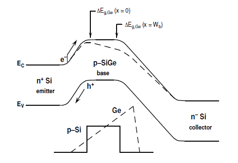
Figure 1: Band diagram of a graded base SiGe HBT and a comparatively constructed Si BJT.
Consequently,
For the same base-emitter voltage, this results in a higher collector current and hence a higher beta dc wise, and a smaller transit time and hence a higher cut-off frequency fT.
Beta is often more than sufficient and can be traded for smaller base resistance, which will then decrease transistor input power consumption, as the input current has to flow through the base resistance. This results in higher power gain, as measured by the maximum oscillation frequency fmax.
A higher beta, a higher current gain, and a lower base resistance all help the transistor maintain a high signal to noise ratio when used as amplifiers, as measured by the low noise figure.
A graded base also helps to make the collector current less sensitive to base width modulation by collector voltage, simply because the minority carrier concentration integral is dominated by the lower Ge regions near the emitter, as measured by the much higher output impedance or Early voltage.