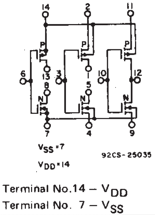
The CD4007 consists of 3 pairs of complimentary MOSFETs, as shown in figure 1.
Each pair shares a common gate (pins 6,3,10).
The substrates of all PMOSFETs are common (pin 14),
as well as those of the NMOSFETs (pin 7).
For the left pair, one of the two NMOS N+ terminals
is tied to the NMOS substrate, and one of the two PMOS P+
terminals is tied to PMOS substrate.
The other two pairs are more general purpose.
For the right pair, a N+ terminal of the NMOS is tied to a P+ terminal
of the PMOS (pin 12).
The CD4007 is a very versatile IC with many uses.
For example, a single CD4007 can be used to make a
chain of 3 inverters,
an inverter plus two transmission gates,
or a complex logic gate.
Inverters and transmission gates
are particularly useful for building D flip-flops.
While the CD4007 is very versatile,
it is also easily damaged by static, like all CMOS electronics.
The CD4007 includes diodes to protect it from
static discharge, but it can still be damaged
if it is not handled carefully.
Normally one would use anti-static
mats and wrist straps when working with
static sensitive electronics.
However, we do not have those in the 2210 lab.
A low budget way to avoid static discharge is to ground yourself before touching an IC. The ELVIS breadboard includes a metal pad in both top corners labeled “ESD PAD TOUCH TO DISCHARGE.” Discharging any built up static charge before picking up a CD4007 will help ensure that you do not have a broken chip half way through the lab.
When specifying wiring between the pins of an IC,
engineers often use a shorthand for connections.
For example, instead of saying, “connect pin 22 to pin 5 and pin 7,”
one might write “(22,5,7)”.
Groups of pins that are not connected are separated by a semicolon.
For example, consider (22,5,7);(1,3,18).
This notation is often used in datasheets, and is used below as well.
Draw an equivalent circuit for the following wiring description using a CD4007:
(1,5,10);(3,8,13);(14,2,11);(7,4,9);(14,Vdd);(7,Ground).
You do not have to draw a gate level schematic if you can determine the logic function implemented.
If you only give a logic diagram, show pin numbers between logic elements.
Make a pin-level wiring diagram for a transmission gate using a CD4007.
Use the top right PMOSFET and the bottom center NMOSFET shown in figure 2 below.
Determine the logic function implemented by the following connections to a CD4007:
(2,14);(8,9,4);(12,13,5);(1,11);(14,Vdd);(7,Gnd). Pin 3 is A, pin 10 is B, and pin 6 is C. The output is pin 12,13, or 5.
Draw a transistor level diagram and a truth table for the circuit.
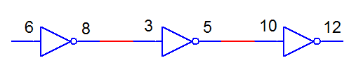
Construct 3 inverters using a CD4007 by making the following connections:
(4,9,7);(1,5);(8,13);(14,2,11);(14,Vdd);(7,Ground).
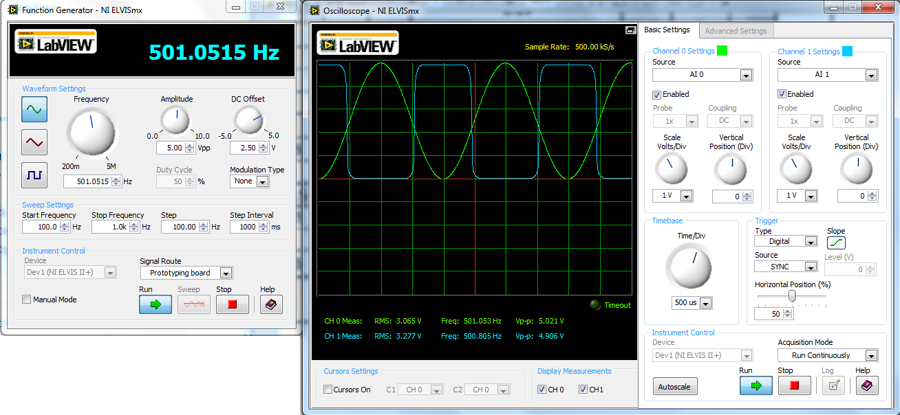
Use +5v for Vdd. Connect AI0+ to FGEN. Set the function generator to output a 500Hz sine wave, 5vpp, 2.5vdc offset.
Test each inverter by connecting the function generator to the input and connecting AI1+ to the output.
Remember to ground the AI- terminals.
The respective input-output pairs are: 6-8,3-5,10-12.
You should see 3 waveforms similar to the one shown in figure 3.
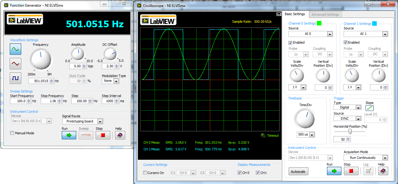
Keeping the input (from FGEN) at pin 6, connect AI1+ to the output of each inverter (one-after-another) and take a screenshot similar to figure 5. You should take a total of three screenshots, one each, corresponding to each inverter output.
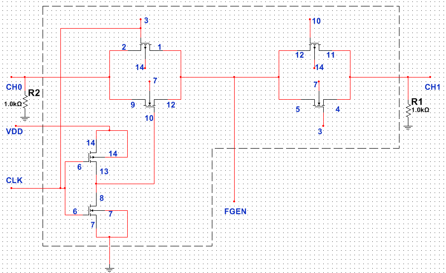
Build a double transmission gate using a new CD4007 chip as shown in Figure 6. We will test the two transmission gates by connecting FGEN to the input, and connecting a load of 1k on either (output) sides.
Connect FGEN to (1,12,5); attach 1k resistors to (2,9) and (4,11) as shown in Figure 6.
Connect pins (2,9) to CH0, and pins (4,11) to CH1. Remember to ground the CH(-) terminals.
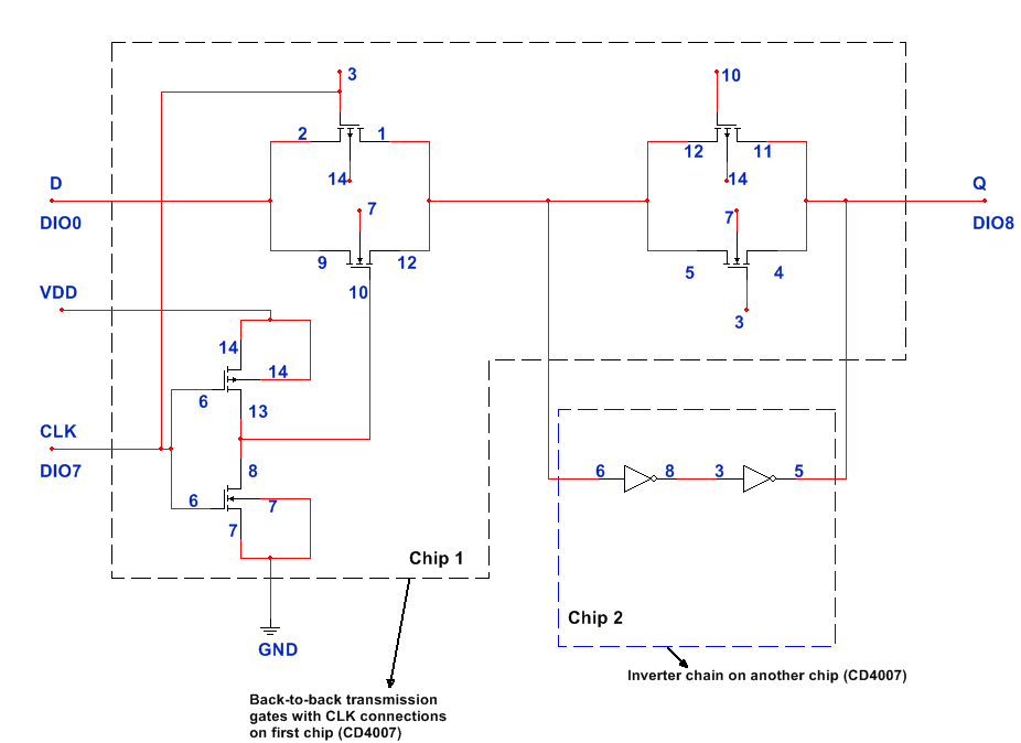
We will now combine the double transmission gate built in the previous exercise with inverter chain of the first exercise to build a D-latch as shown in Figure 7. The two transmission gates work in tandem to realize the D-latch. During the transparent phase of the latch, i.e. CLK=0, the first transmission gate (left) is ON while the second (right) is OFF. D is transmitted to the output (Q) through the first transmission gate and the two-inverter cascade. During the hold phase of the latch, i.e. CLK=1, the first transmission gate is OFF but the second transmission gate is ON. As a result, any change in the input D is not reflected at the output Q. However, the second transmission gate, which is now turned ON ensures that the previous logic level at Q is retained through the closed loop with the two-inverter cascade.
Connect pin 9, which serves as D input of the latch to DIO0. Connect pin 4, which serves as Q output of the latch to DIO8. Connect pin 6, which serves as CLK to DIO7.
Now insert two inverter chain you built earlier (and retained from the first exercise) to the circuit you have just built. It is shown in the dashed box labeled as chip 2 in Figure 7 above.
First apply logic Low to CLK by starting the SFP and turning DIO7 low. Apply logic High to the D input by flipping DIO0 to high.
Observe the output Q of the latch on DIO8 (by using the digital reader from the SFP). A steady high should appear. Capture a screen shot.
Apply logic Low to the D input by flipping DIO0 to low. Observe the output on DIO8. This is the transparent phase of the latch. You should see that DIO8 is also low.
Now apply logic High to CLK by making DIO7 high. Also apply logic High to the D input.
Observe the DIO8 pin. A steady low should appear inspite of changing D to logic High since the previous value at D-input was low. Capture a screen shot. This is the opaque phase of the latch.
Two copies with opposite phase clocks will then make a master-slave D Flip Flop.
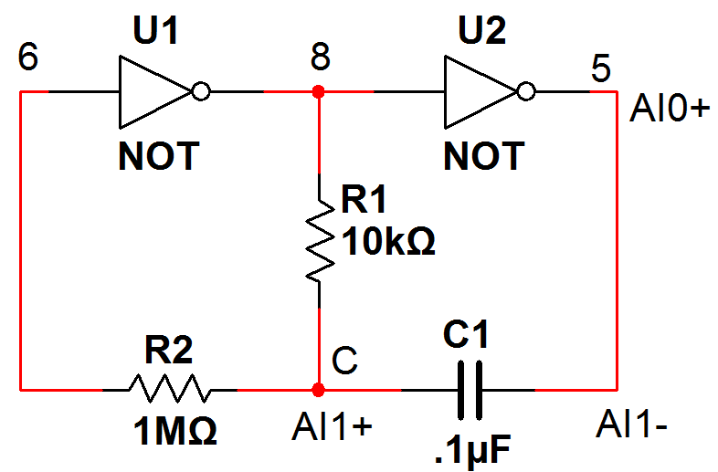
First, assume the voltage at the input to the first inverter is zero. The output of the first inverter will be Vdd and the output of the second inverter will be zero. The capacitor will begin to charge. Because the input to a CMOS inverter is very high impedance, the resistor R2 can be ignored. Thus, the input to the first inverter is close to the voltage at node C. When node C reaches 1/2 Vdd, the inverters will change states, and the voltage at the output of the second inverter will now be Vdd. Because the voltage across the capacitor cannot change quickly, the voltage at the bottom center node will now be Vdd + Vcap, or about 3/2 Vdd. Because the output of the first inverter is now zero, the capacitor will begin to discharge through R1, and the opposite side will be charged. When the voltage at node C drops to 1/2 Vdd (making the voltage across the capacitor -1/2 Vdd), the inverters will change states. The output of the second inverter will be 0v again, and the voltage at node C will now be 0 + Vcap or 0 -1/2 Vdd. The capacitor will begin to charge through R1 until node C reaches 1/2 Vdd and the process repeats.
In summary, the output of the inverters will oscillate between 0 and Vdd. Therefore, this circuit is an oscillator.
Construct the circuit shown in figure 8. The two inverters can be built from a CD4007 by making the following connections: (4,7);(1,5);(3,8,13);(14,2);(14,Vdd);(7,Ground). You may find the diagram shown below in figure 9 helpful.

 on either (output) sides.