3. Two Terminal MOS
3.1. Notes
2-terminal MOS updated 2/7 Download.
2-T MOS inversion charge updated 2/7 Download.
Read this before Th. class, and practice generating plots. We went over some of these in the past, but we now have a better understanding and more tools you can use.
I in general spend lots of time revising / creating new notes, so notes will likely be updated, but you are still encouraged to look through these notes before lecture for best result of learning.
Capacitances updated 2/7 Download.
3.2. Homeworks
Put your homework solution codes and graphics into a word, latex, or html document. Do this for all homeworks. I’d like you to submit your homeworks to me on Thursday.
(1/24) Write a program with Matlab or Python that calculates the surface charge as a function of surface potential for p-type substrate.
Observe the special points, 0, fermi potential, twice fermi potential. Generate some plots, save it.
Try the special case of N+ poly gate, 30nm oxide, 5e15cm-3 substrate doping. I will provide sample plots for this case for you to compare against.
(1/26) Run the new programs provided today (always download the latest version). I have made some improvements to figures generated by the Nmos.plot() method. Write some additional codes based on what you learned today to generate plots for:
- doping = 1e16, 1e17, 5e17, all with tox = 2nm
- tox = 1nm, 2nm, 10nm, all with doping = 1e17
Make comparisons and observations on the impact of doping and tox. Put them in a word or latex document, or a powerpoint document.
At present, additional coding is needed to overlay curves from different doping or tox. You are not required to do so. Just use the Nmos.plot() method for now. You can still a great deal of information by looking at these plots.
(1/31) Repeat the previous homework using the new version of the python codes. They can handle Vcb now as well. But if you do not specify Vcb, it defaults to zero.
You may use the mos_doping_impact() and mos_list_demo() codes as template for this exercise.
- Download and save as equisemi.py.
- Download and save as nmos_demo.py.
- Download and save as myplot.py.
I had to deal with several numerical issues (finite computer resolution induced errors mainly), which took up lots of time. It took up more than 8 hours per day since last Thursday to get everything working in a way I hope that will allow you to make little change to the code to generate plots of your own.
I can make a GUI with QT, but I feel you are better off with writing a few lines of scripts to iterate over any list of structures you want.
To generate a list of Mos with 2nm tox, with a few doping levels at irregular step, just type in a list of dopings (as opposed to using np.logspace before):
def mos_doping_impact():
    '''sample home work problem on doping impact'''

    # create a metal, an oxide and a ptype semi
    metal = Metal('Npoly')
    oxide = Oxide(2)
    dopings = [1e16, 1e17, 5e17]
    nmos_list = []

    for doping in dopings:
        psemi = Psemi(doping)
        nmos = Nmos(metal, oxide, psemi)
        nmos_list.append(nmos)

    NmosPlotter(nmos_list)
We create an empty list nmos_list, and then add nmos objects to it by the append method when looping over all the doping in the list dopings.
In the end, we create a NmosPlotter with the nmos_list - which will automatically take care of the plotting.
Look for the .png files on disk, you can also save the graphs you see on screen by clicking the disk icon. This is useful if you make modifications to the plots, e.g. zooming into a particular area to better see special points of interest.
(1/31, optional) Practice using fsolve in matlab or python, or the bisect method we discussed today to solve surface potential versus Vg. You may try this just for one or two biases to get a feel of how it works. For bisect, just use the code provided, which I modified from algorithms in a numerical computing book.
I have provided you with my codes and explained how to do this in python. Read the relevant functions / codes in the equisemi.py and nmos_demo.py files. You do not need to precisely understand the plotting codes, but should understand the calculation codes.
(1/31) Using the codes I provide, plot out surface potential, total Si charge and inversion charge versus Vg from -1V to 2V, for tox=5nm, doping=1e17cm-3. Use Vcb=0V for now (default if not specified).
Use the ps_bisect_demo() as a template for your own exploration. The codes are listed below:
def ps_bisect_demo():
    '''demo for calculating surface potential for given gate voltage with multiple Vcb using bisect method'''
    nmos = Nmos()
    vg = np.linspace(-2, 2, 100)
    ps = vg.copy()
    qinv = vg.copy()

    ps_from_vg = nmos.ps_from_vg_bisect
    qinv_from_ps = nmos.qinv_from_ps

    vcbs = [0, 0.5, 1.0]
    cols = colors[:]
    ax = None
    ax_qinv = None

    for vcb in vcbs:
        nmos.vcb = vcb
        color = cols.pop(0)
        for idx, vg_item in enumerate(vg):
            ps[idx] = ps_from_vg(vg_item)
            qinv[idx] = qinv_from_ps(ps[idx])

        line, ax, fig = myplot(ax = ax, x = vg, y = ps, \
                              xlabel = '$V_g (V)$', \
                              ylabel = '$\phi_{s} (V)$', \
                              label = 'vcb=%4.1f' % (vcb), \
                              color = color)

        line, ax_qinv, fig_qinv = myplot(ax = ax_qinv, x = vg, y = qinv, \
                              xlabel = '$V_g (V)$', \
                              ylabel = '$Q_{inv} (C/cm^2)$', \
                              label = 'vcb=%4.1f' % (vcb), \
                              color = color)

        cols.append(color)

        fig.savefig(nmos.name+'_ps_from_vg_bisect.png', format=fig_format)
        fig_qinv.savefig(nmos.name+'qinv_from_vg_bisect.png', format=fig_format)
Running this program results in these two graphs:
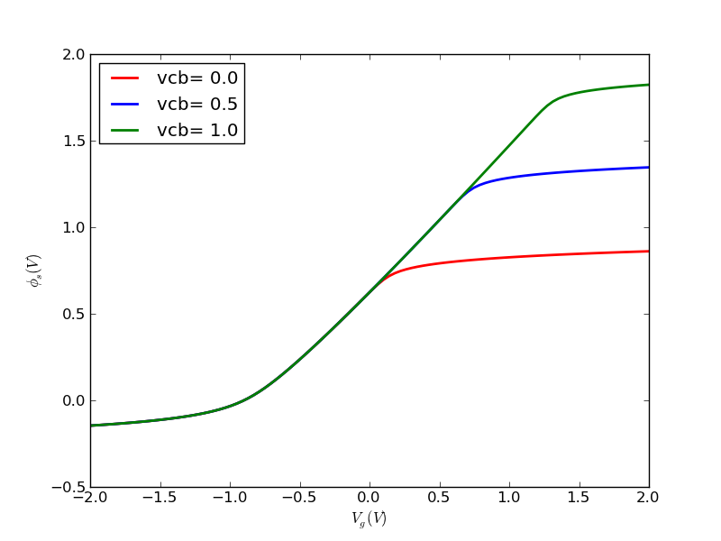
Figure 1: Surface potential vs gate voltage for various Vcb’s. tox = 30.00 nm, Nsub=5e+15 cm-3. Bisect method is used.
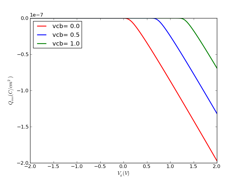
Figure 2: Inversion charge vs gate voltage for various Vcb’s. tox = 30.00 nm, Nsub=5e+15 cm-3. Bisect method is used.
(2/2) Update the codes. Fang has had tremendous trouble with downloading latest file, even with Ctrl+R. IE did the correct job in the end.
The new codes provide more plots. Examine the new plots.
Using the new techniques you learned today, write a few more functions / programs to look at doping and oxide dependence, even manually creating a list of nmos.
Practice using HDFview on the files generated too.
3.3. Source Codes
- Updated 1/31 5:30pm, supporting list, vcb, and solving surface potential from vg.
- Updated ** 1/26 *
new feature: title is added to plots generated by nmos.plot()
new feature: png file is now named with the tox and Na values as file prefix.
Note: period in file name is not generally used in windows, so I used ‘p’ instead.
3.3.1. Install the decorator package
Open a windows cmd command window, type:
cd c:\python27\scripts
easy_install.exe decorator
This will download and install the decorator package.
3.3.2. Download Modules
3.4. Sample Plots
3.4.1. 30nm, 5e15cm-3

Figure 3: Qs and Qs without n vs surface potential tox = 30.00 nm, Nsub=5e+15 cm-3
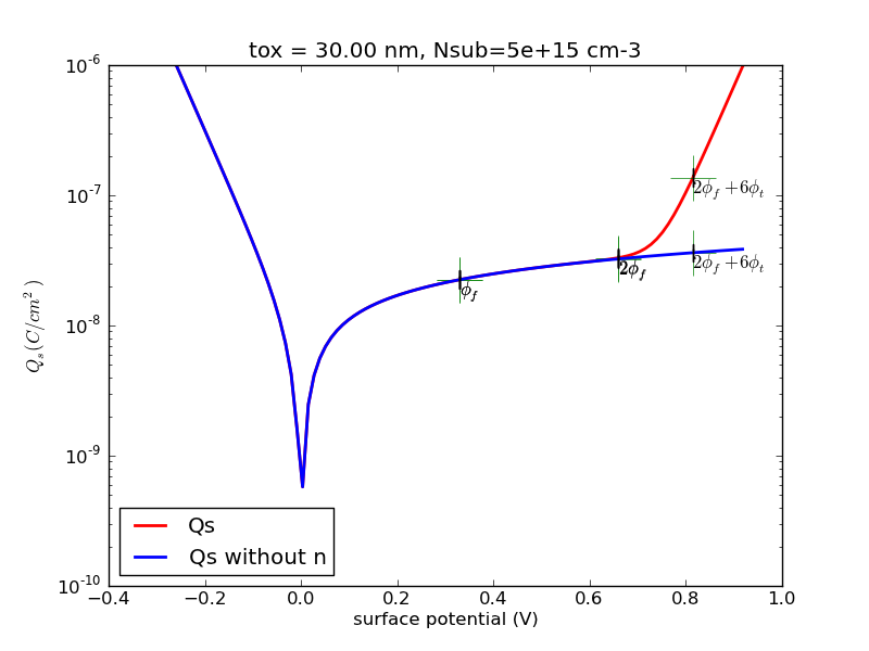
Figure 4: Log scale Qs and Qs without n vs surface potential tox = 30.00 nm, Nsub=5e+15 cm-3
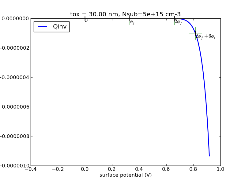
Figure 5: Qinv vs surface potential tox = 30.00 nm, Nsub=5e+15 cm-3
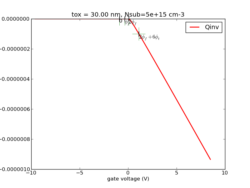
Figure 6: Qinv vs gate voltage tox = 30.00 nm, Nsub=5e+15 cm-3
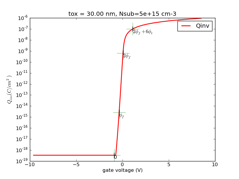
Figure 7: Log scale Qinv vs gate voltage tox = 30.00 nm, Nsub=5e+15 cm-3
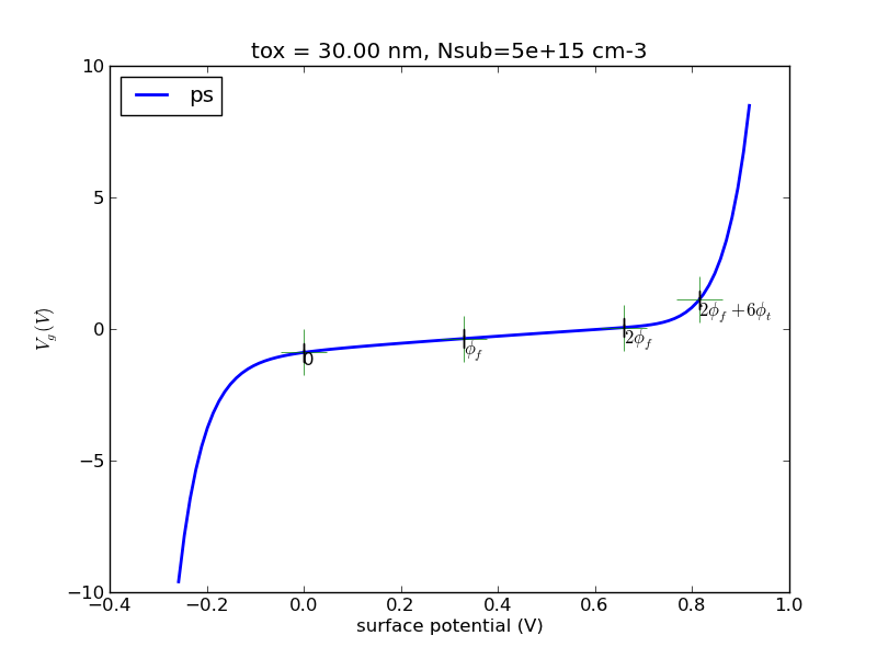
Figure 8: Log scale Qinv vs gate voltage tox = 30.00 nm, Nsub=5e+15 cm-3
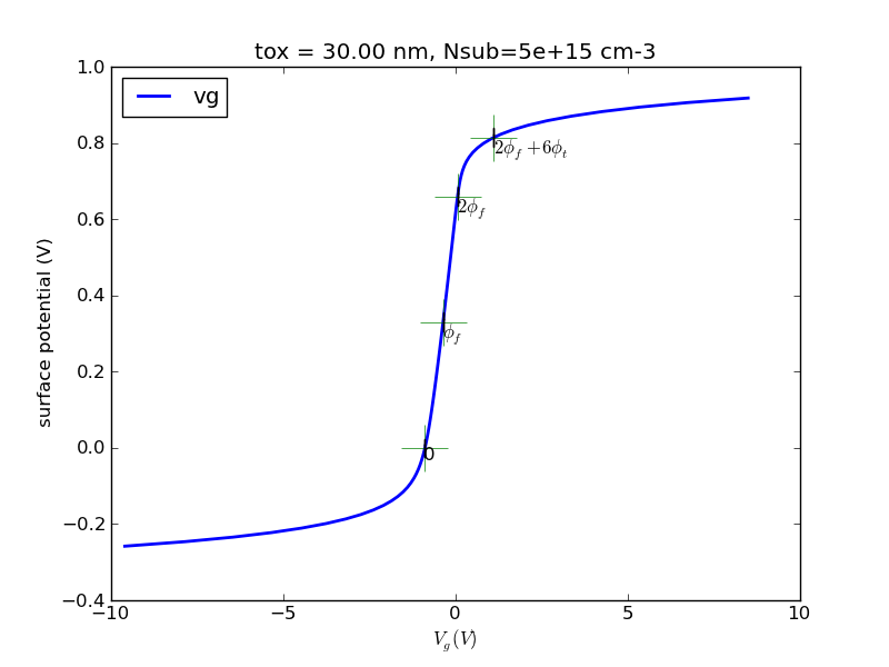
Figure 9: Surface potential vs gate voltage tox = 30.00 nm, Nsub=5e+15 cm-3
3.4.2. 2nm, 5e17 cm-3

Figure 10: Qs and Qs without n vs surface potential tox = 2.00 nm, Nsub=5e+17 cm-3

Figure 11: Log scale Qs and Qs without n vs surface potential tox = 2.00 nm, Nsub=5e+17 cm-3
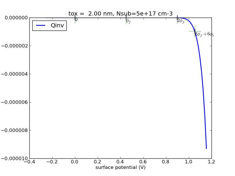
Figure 12: Qinv vs surface potential tox = 2.00 nm, Nsub=5e+17 cm-3
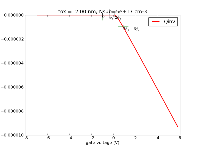
Figure 13: Qinv vs gate voltage tox = 2.00 nm, Nsub=5e+17 cm-3
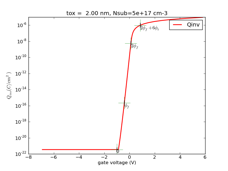
Figure 14: Log scale Qinv vs gate voltage tox = 2.00 nm, Nsub=5e+17 cm-3
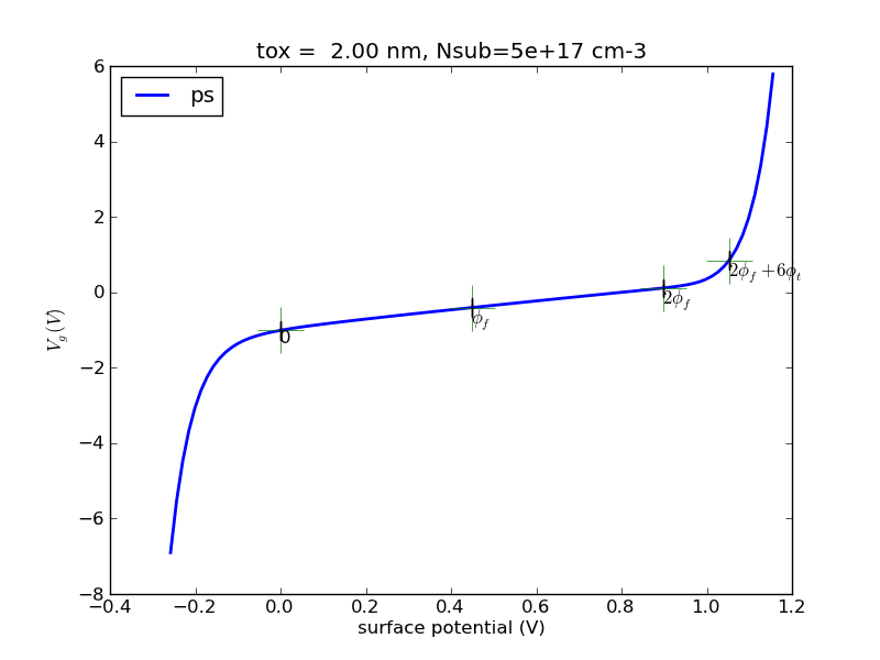
Figure 15: Log scale Qinv vs gate voltage tox = 2.00 nm, Nsub=5e+17 cm-3
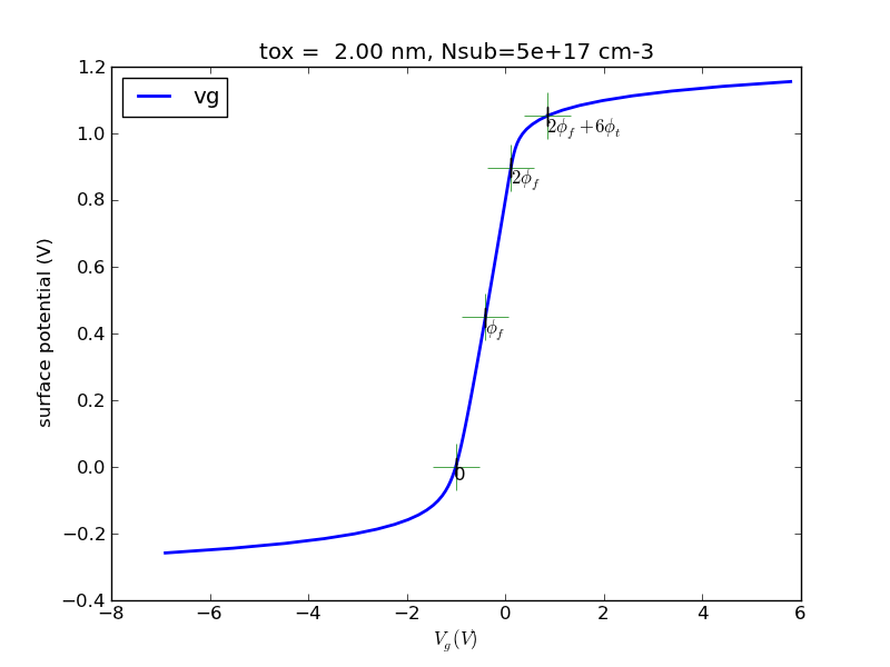
Figure 16: Surface potential vs gate voltage tox = 2.00 nm, Nsub=5e+17 cm-3