SiGe Device Example 02
This is our second Sentaurus example on SiGe/Si double heterojunction devices. It builds upon the 1st example. Again, we are mimicing the p-type SiGe base of a SiGe HBT. The dimensions and parameters are exaggerated for ease of handling. We will, however, use more realistic structural parameters as found in state-of-the-art hundreds of GHz speed HBTs in our homeworks. The new features / functions to learn are:
- Examination of fundamental outputs with more options in the Plot section.
- Placement of multiple grid refinements. Here only a fine regridding based on heterojunction locations is made.
- Use of the Eval function to specify xMoleFraction or dopant concentrations.
For now, let us not worry about applying biases and only focus on the equilibrium solution. We will show later on how the equilibrium solution determines HBT’s collector current and base transit time by deriving the famous Kromer’s two integral relationships pertaining to the operation of HBTs.
Note
Kromer won a Nobel Physics Prize for his contribution to heterojunction devices.
Boundary
First the boundary file. You can download the file here
SiliconGermanium "substrate" {line [(0) (1)]}
SiliconGermanium "epi" { line [(1) (1.2)] }
Contact "pcontact" { point [1.2] }
Contact "ncontact" { point [0] }
Here is a note
Note
See our Word docx file for additional explanations on why two sections are used, and why SiliconGermanium is used for both the substrate and epi layers.
Mesh command file
The mesh command file can be downloaded here. There are two sections, definition and placement. In the definitions, we define
- AnalyticalProfile "Profile.Ge" using the Eval function.
- AnalyticalProfile "Ge.external" using subMesh1D function to read in an external Ge file.
- Refinement "R.Fine"
- Refinement "R.Global"
- Constant N doping "Const.N"
- Constant P doping "Const.P"
- Implantation p-type doping "ImplantP.profile"
Definitions
{

        AnalyticalProfile "Profile.Ge"
        {
          Species = "xMoleFraction"
          Function = Eval(init="a=0.5", function="0+a*x", value = 0)
        }

        AnalyticalProfile "Ge.external"
        {
                Function = subMesh1D(Datafile = "mole.txt" , Scale = 1, range= line [(0, 0) (1, 0.1)])
                LateralFunction = Erf(Factor = 0)
        }


  Refinement "R.Fine"
  {
        MaxElementSize = (0.004)
        MinElementSize = (0.002)
  }

  Refinement "R.Global"
  {
        MaxElementSize = (0.02)
        MinElementSize = (0.01 )
 ##   RefineFunction = MaxTransDiff(Variable = "DopingConcentration", Value = 1)
  }

  Constant "Const.N"
  {
        Species = "ArsenicConcentration"
        Value = 1e+17
  }


  Constant "Const.P"
  {
        Species = "BoronConcentration"
        Value = 1e+17
  }

 Constant "Const.Ge"
  {
        Species = "xMoleFraction"
        Value = 0.1
  }

  AnalyticalProfile "ImplantP.profile"
  {
        Species = "BoronConcentration"
        Function = Gauss(PeakPos = 0, PeakVal = 1e+20, ValueAtDepth = 1e+17, Depth = 0.5)
  }


}
Next, we place these definitions in different regions of the heterojunction structure. Pay attention to ReferenceElement, EvaluateWindow and use of R.Fine and R.Global. I strongly encourage you to change the values of all relevant parameters, observe output in tecplot_sv, so that you can better understand the meanings of these commands.
Note
The same commands are used in our future 2-D and 3-D designs as well. The main difference is that in 2-D, ReferenceElement is a line, and in 3-D, a polygon. The lateral extension will also need to be specified in 2-D and 3-D cases.
Placements
{
  Refinement "RP.Global"
  {
        Reference = "R.Global"
  }

  Refinement "RP.Fine"
  {
        Reference = "R.Fine"
        RefineWindow = line [( 0.19) , (0.21 )]
  }

  Refinement "RP.Fine"
  {
        Reference = "R.Fine"
        RefineWindow = line [( 0.69) , (0.71 )]
  }

  Constant "PlaceCD.background"
  {
        Reference = "Const.P"
  }

#  Constant "PlaceGe.Const"
#   {
#       Reference = "Const.Ge"
#    EvaluateWindow
#       {
#    Element = line [( 0 ) , ( 0.5 )]
#       }
#   }


  AnalyticalProfile "PlaceGe Profile"
  {
  Reference = "Profile.Ge"
        ReferenceElement
        {
          Element = point[( 0 )]
          Direction = positive
        }
        EvaluateWindow
        {
          Element = line [( 0.2 ) , (0.7)]
        }
}

}
The numbers are chosen for easy handling. You should try to observe why certain values are used. For instance:
Refinement "RP.Fine"
{
      Reference = "R.Fine"
      RefineWindow = line [( 0.69) , (0.71 )]
}
Here the RefineWindow covers the 2nd SiGe/Si heterojunction. If you were to use line [( 0.75) , (0.78 )], the result will look different - you should realize why that is not desired.
The two numbers 0.69 and 0.71 came from the Ge profile placement:
  AnalyticalProfile "PlaceGe Profile"
  {
  Reference = "Profile.Ge"
        ReferenceElement
        {
          Element = point[( 0 )]
          Direction = positive
        }
        EvaluateWindow
        {
          Element = line [( 0.2 ) , (0.7)]
        }
}
Note that the second SiGe/Si heterojunction occurs at 0.7, as our reference element is at x = 0.
Note
It is always a good idea to inspect the structural integrity of your simulated device before running sdevice. Using tecplot, check boundary of each material and named region, doping profile, and Ge profile against what you had in mind. Any obvious meshing problem can also be discovered at this point.
Sdevice command file
The sdevice command file can be downloaded here.
Device MySiGeResistor
        {
        Electrode
        {
                { Name="pcontact"    Voltage=0.0 }
                { Name="ncontact"     Voltage=0.0}
        }

        File
        {
          Grid    = "n10_msh.grd"
          Doping = "n10_msh.dat"
          Current = "n10_des.plt"
          Plot    = "n10_des.dat"

        }

        Physics
        {
                Temperature=300


                 Mobility
                        (
                                PhuMob(Phosphorus)
                        )
        }
        Plot
        {
                eDensity hDensity
                eCurrent/Vector hCurrent/Vector
                TotalCurrent/Vector
                eQuasiFermi hQuasiFermi
                eGradQuasiFermi hGradQuasiFermi
                eVelocity hVelocity
                eMobility hMobility
                ElectricField
                Potential
                SpaceCharge
                DopingConcentration DonorConcentration AcceptorConcentration
                ConductionBand ValenceBand
                Bandgap                 EffectiveBandGap
                eEffectiveStateDensity          hEffectiveStateDensity
                EffectiveIntrinsicDensity
                xMoleFraction
                eMobility hMobility
        }


}

Math
{
          Extrapolate
          RelErrControl
          Notdamped=50
          Iterations=20
}

File
{
          Output    = "n10_des.log"
          ACExtract = "n10_ac_des.plt"
          Plot = "n10_des.plt"
}

System
{

          MySiGeResistor R1 (pcontact=positive ncontact=negative)
          Vsource_pset vp (positive 0) {dc=0}
          Vsource_pset vn (negative 0) {dc=0}
}

Solve
{
          Poisson
          Coupled { Poisson Electron Hole }


          Quasistationary (
                                          InitialStep=0.01 MaxStep=0.1 Minstep=1.e-5 increment=1
                                          Goal { Parameter=vp.dc Voltage=1 }
                                          Plot{    Range=(0 1) Intervals=5 }
                                          )
                                          {
                                                ACCoupled
                                                (
                                                  StartFrequency=1e3 EndFrequency=1e3
                                                  NumberOfPoints=1 Decade
                                                  Node(positive negative) Exclude(vp vn)
                                                )
                                                {
                                                  Poisson Electron Hole
                                                }
                                          }
}
Warning
The word Plot has numerous meanings in Sentaurus device. Observe your output files as your run simulations, you will better understand what type of “plot” is referred to.
For this week’s homework, pretty much all the relevant “Plots” of internal position dependent variables are requested in the Plot section.
Plot
{
        eDensity hDensity
        eCurrent/Vector hCurrent/Vector
        TotalCurrent/Vector
        eQuasiFermi hQuasiFermi
        eGradQuasiFermi hGradQuasiFermi
        eVelocity hVelocity
        eMobility hMobility
        ElectricField
        Potential
        SpaceCharge
        DopingConcentration DonorConcentration AcceptorConcentration
        ConductionBand ValenceBand
        Bandgap                 EffectiveBandGap
        eEffectiveStateDensity          hEffectiveStateDensity
        EffectiveIntrinsicDensity
        xMoleFraction
        eMobility hMobility
}
The meanings of most of these keywords are obvious, except for
- EffectiveBandgap means the effective bangap after bandgap narrowing due to heavy doping is accounted for.
- ElectricField and SpaceCharge are absolute values, the sign is not included. Additional specifications are needed to obtain vector (signed x, y, and z components).
Sample outputs
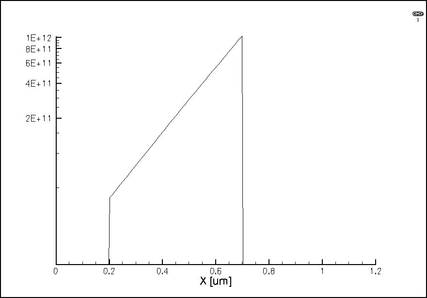
EffectiveIntrinsicDensity.
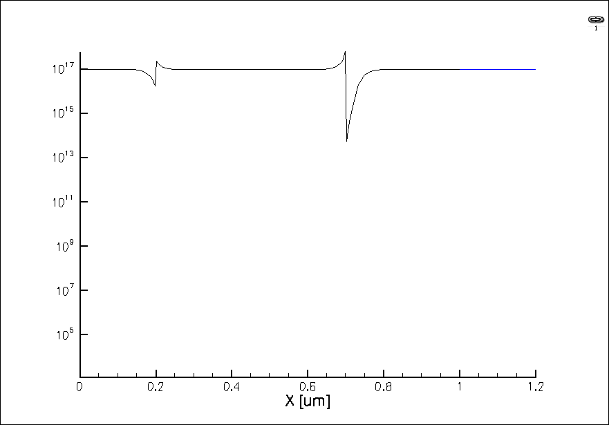
Hole density.
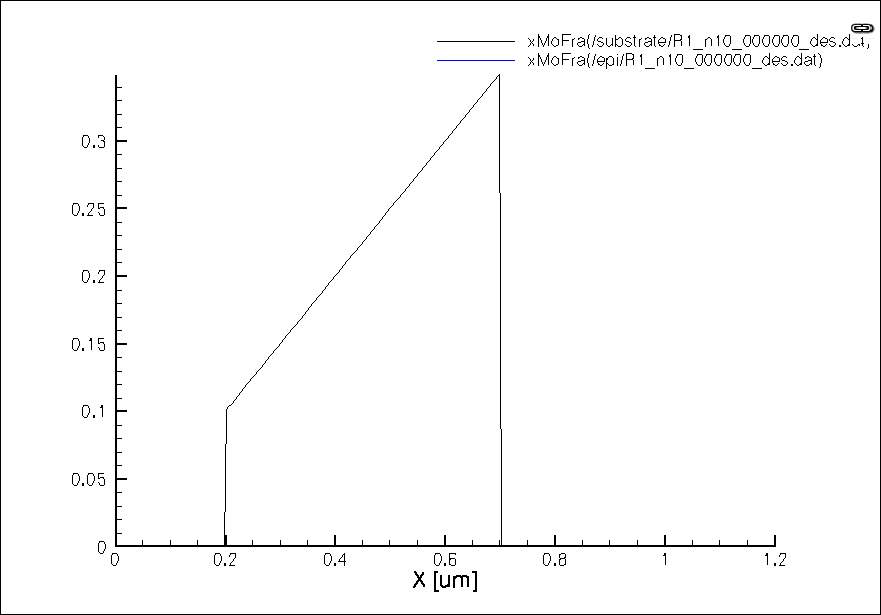
Ge Mole fraction.
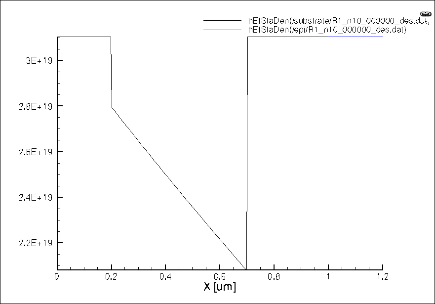
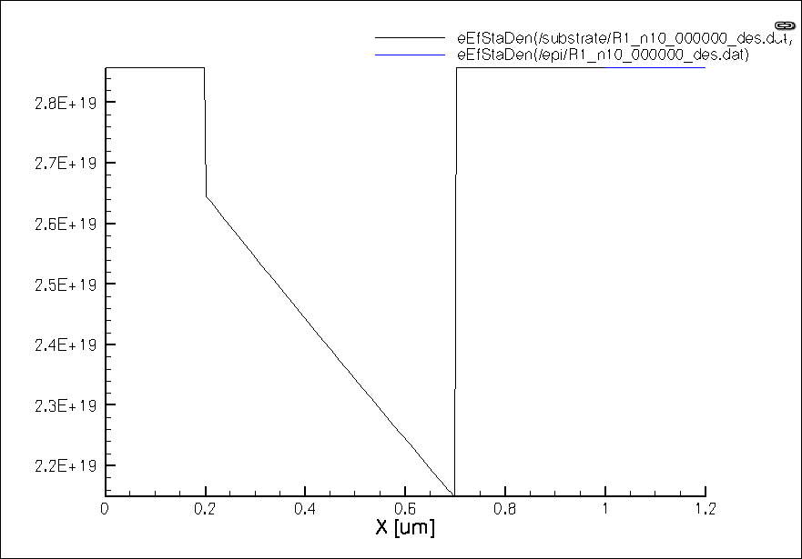
Nv - Valence band density of states.
Nc. Conduction band density of states.