Etec pattern exposed on a substrate of 500 nm PMMA on Si
(Click on the image to see detail)
Center Region
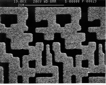
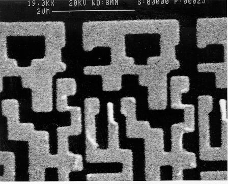
Uncorrected Pattern Corrected Pattern
Edge Region
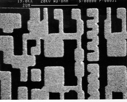
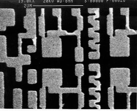
Uncorrected Pattern Corrected Pattern

| SHAPE CORRECTION |
|---|
| FEATURES |
|---|
The first version of PYRAMID adjusts shapes of circuit primitives for correction of proximity effect.
Rule-tables are used to speed up correction.
It employs a two-level hierarchy of correction to be general and fast.
Fast but accurate estimation of exposure is possible due to decomposition of exposure into local and global components and use of the CDF table.
PYRAMID has been shown to be able to correct various circuits with minimum feature size down to 0.1 um, and to be faster than other schemes.
It is compatible with not only raster or vector scan machines but also shaped-beam machines.
It is the only practical proximity effect correction method for a massively parallel E-beam machine.
| EXPERIMENTAL RESULTS |
|---|
Uncorrected Pattern Corrected Pattern
Uncorrected Pattern Corrected Pattern