4. Virtual Breadbording and Correctness Verification
For circuits that we will build and test using ELVIS II+, I would like you to try a new way of circuit simulation. Instead of creating a regular general purpose design, we can create a design specifically for use with ELVIS.
This approach has a number of advantages:
- You will use the same instruments as found on the ELVIS board in simulation. You will no longer need to place these instruments as components. You just need to wire them.
- You can do virtual breadboarding before the physical lab.
- You can verify correctness of your virtual breadboarding using the program’s internal design rule checker (DRC) and layout versus schematic (LVS) checker.
4.1. Goal
- Learn how to create ELVIS design
- Learn how to do virtual breadboarding
- Learn how to use design rule and connectivity checker to help achieve correct breadboarding
4.2. Prior Tutorials Required
The BJT tutorial. See Multisim Tutorial Using Bipolar Transistor Circuit.
The Rectifiers tutorial. see Rectifiers Simulation with Scope Instrument.
4.3. Create an ELVIS II Design
To create an ELVIS II design, from main menu, select File -> New ELVIS II Design.
The rest of the procedure is quite straightfoward and very similar to the usual schematic capture, except that we will use ELVIS board instruments directly by wiring to the built-in pin sockets on a virtual Elvis schematic design sheet.
The virtual schematic sheet contains a number of items that correspond to elements of the physical ELVIS board, and looks like:
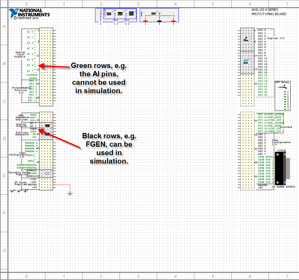
Figure 1: a blank virtual ELVIS design schematic
The rails on the left and right of the main workspace correspond to rails on the actual ELVIS II board, as indicated by the labels.
Instead of placing a AC voltage souce or AC power source from components, we simply use the function generator as our AC source, since that is what we will use in the physical lab to generate the AC signal.
There a number of complications we will address later. For now, do not wire the scope and DMM, which will cause DRC and LVS errors. We will do that after DRC and LVS are successful.
For illustration, we will use a simple circuit, a half wave rectifier we learned earlier. Here is what the circuit looks like:
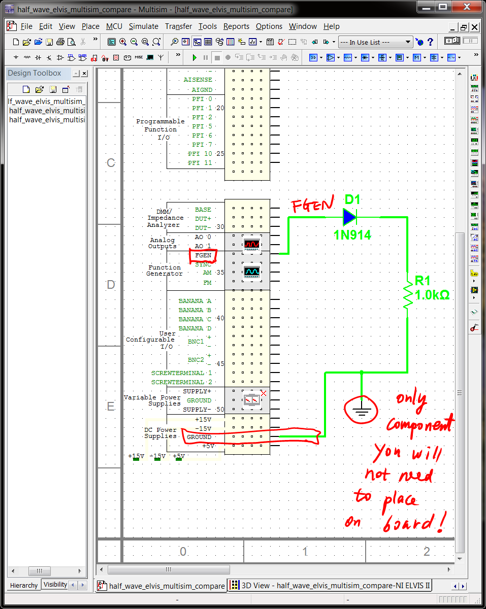
Figure 2: schematic of half wave rectifier as ELVIS II design
4.4. Virtual Breadboarding and Correctness Checking
In main menu, select Tools -> Show Breadboard. You will see a 3-D picture of a virtual ELVIS board:
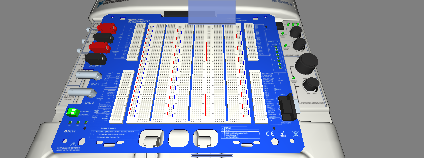
Figure 3: 3D view of the virtual ELVIS board
Follow the on-screen instructions to place components and wires. You can select color for each wire.
There is only one component that does not need to be placed, that is the ground. Instead, all ground should be tied to the GROUND pin of the ELVIS board. A convenient way is to tie the GROUND pin to the blue ground strips.
After you finish the layout, which includes placing components and wiring them up according to your schematic, click the checker icon as shown below. The program will report any design rule and wiring connectivity errors. A successful virtual breadbording looks like this:
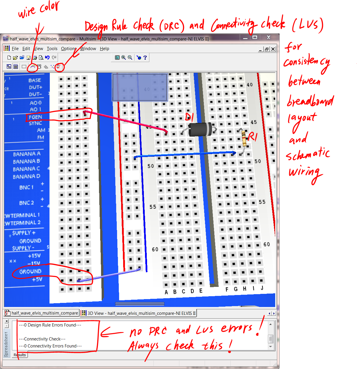
Figure 4: virtual breadboarding, DRC and LVS checking example using half wave rectifier
Once this is successful, you can run your simulation by connecting the interested nodes to the scope, and then click the run button. That process is identical to what we learned earlier, and thus will not be repeated here.
Next, you can use the virtual breadboarding result as a visual reference in building the actual circuit in the physical lab.
By design we use a simple circuit for illustration. You can of course also place more complex ICs as you would on the actual board.
This should also give you a taste of DRC and LVS useful for our discussion of CMOS layout design later in ELEC 2210.
DRC in CMOS IC Design
We will learn more about DRC and LVS later in CMOS IC layout design. For breadboarding, there is not much design rule to worry about, and it is mainly a matter of LVS. In making printed circuit boards, there will be some design rules to follow. In CMOS IC, there are hundreds of design rules circuit designers have to strictly follow.
DRC makes sure that the layout of the part is manufacturable for a given foundry process, e.g. 32nm TSMC CMOS process. For instances, if two metal wires are too close together within the same metal layer, they may become shorted unintentionally during the manufacturing process, because of the finite precision that is inherent in the manufacturing.
How is LVS Done?
LVS checking compares the netlist from the schematic with the netlist from virtual breadboard components placement and wiring. In IC design, LVS compares schematic netlist, often from synthesis, with the netlist from physical layout, e.g. a GDSII layout.