Multisim Tutorial Using Bipolar Transistor Circuit Simulation
updated 2/3, 2012
This is a quick tutorial for teaching students of ELEC 2210 how to use Multisim for bipolar transistor circuit simulation. It is written such that no prior Multisim knowledge is required.
My experience with teaching SPICE and Multisim in ELEC2210 is that live tutorials done in class turned out to be most effective compared to written tutorial and video tutorials, and that is what we will rely on in the later part of this class for CMOS circuits. I will still provide screenshots embedded in the journal notes of relevant chapters.
With Multisim, there is not a free version, this makes teaching in classroom more difficult. If you have purchased student version, you can bring your laptop to class.
Multisim is available in ECE 308 and 310 computer labs, with Elvis drivers. It is also available in the basement college of engineering computer labs, but without the Elvis drivers. This likely means all other engineering computer labs should also have it, e.g. in Shelby or Aerospace labs.
It is in some case easier to use than other SPICE based simulators, e.g. Pspice, but can be harder to use in other cases. So in 2210, the plan is to teach both NI Multisim and Cadence Pspice. One practical reason for using Multisim is that it supports virtual instruments simulation, which will be useful as we are also upgrading our 2210 labs with the new NI ELVIS II+ prototype circuit board.
Goal
- Introduction to using Multisim for SPICE like circuit simulation
- Schematic capture
- Analysis setup with DC sweep examples
- Nested sweeps (use source 2)
- Output inspection using grapher
- Bipolar transistor model parameter editing
- Understand bipolar transistor I-V characteristics
Required Prior Multisim Tutorials
None.
Getting Started
First, launch Multisim from programs - this will vary depending on your PC configuration, an example of starting Multisim is given below:

Figure 1: start Multisim
The design environment should pop up as follows:

Figure 2: menus of Multisim design environment
A new design file, with a default named “Design 1”, is created with a blank schematic sheet, also named “Design 1”. On the left is the navigation pane.
Note the standard components toolbars, the virtual components toolbar, and the virtual instruments toolbars. For teaching purpose, we will first use virtual components. Unfortunately, by default, the virtual components toolbar is not shown, so we will need to turn that on as follows:
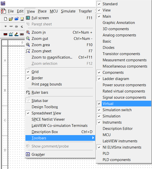
Figure 3: turn on virtual components toolbar
These toolbars will come in handy in placing components, and save a lot of typing, scrolling, searching and clicking.
Schematic Capture
Placing Components
Real versus Virtual Components
Any part that can be placed onto the schematic is called a component. There are real as well as virtual components:
- real component is tied to a part you can buy, and they have properties that cannot be changed, e.g. beta of a transistor. They also have a known and fixed physical size, which will be important to consider if we were to build a printed-circuit-board (PCB). We will need to use real component when simulating a circuit with a part we use in the physical lab, e.g. the 2N3904 bipolar transistor.
- virtual component is for simulation only. For instance, a virtual transistor can have any beta, e.g. 100, 200, or 10, or 4.2210 is we so wish. We can simulate designs with continuous even hypothetical values of parameters. Virtual component is also particularly useful for learning and teaching, since we can use simplified model parameters to facilitate comparison between first order theory and circuit simulation.
Procedures
One can in general use the component toolbar for finding components. For this tuorial, let us use the virtual component toolbar.
Let us now place a few components so that we can simulate the output curves of a bipolar transistor.
Place a virtual NPN transistor as follows:

Figure 4: place a virtual NPN transistor
Place a DC current source which we will use to supply base current as follows:

Figure 5: place the base current source
Place a DC voltage source, which we will use to set the collector-to-emitter voltage VCE, as follows:
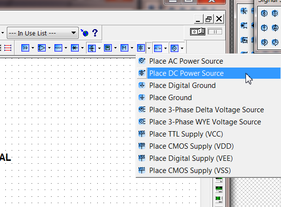
Figure 6: place the VCE dc voltage source
DC Voltage Source is DC Power Source in Multism
The DC voltage source is actually called DC power source. If you had used the search feature, and typed in DC voltage source, the search would have returned no result.
Last but not least, place ground as follows:
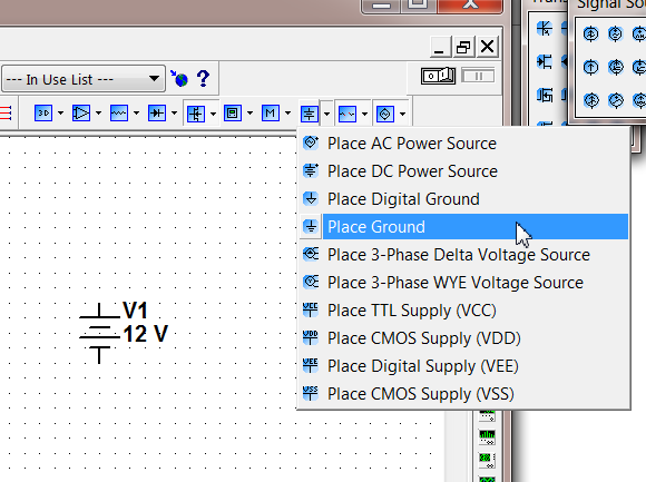
Figure 7: place ground
Always Place Ground!
Ground is under Power_sources in Multisim. Like other SPICE based circuit simulators, it is mandatory to have the proper ground which is the reference point for all the nodal voltages simulated. This ground is known as the 0 node in most SPICE based simulators.
- Select and move around your components to your liking.
- Click a single compoent to select it. Esc to deselect it.
- Hold Shift, then click to select multiple components.
Wiring
Wiring is both particularly simple and particularly difficult in Multisim. The chance is that you will first find the wiring simple or simpler than other programs you used before, at least for simple circuits. When the cursor is close to the unconnected end of any component, it will change into a small black connection dot and crosshair. A click on the end of the component starts the wiring. Move the cursor to where you want it to be connected. The routing of the wire is by default automatic, but manual adjustment is possible.
A very important limitation is that one of the two pins or component ends you are trying to wire together must be unconncted. If both pins are connected, which can easily occur, you will encounter problem of existing connections being broken as new wiring is added. I encoutered the problem within 3 minutes of learning Multisim the first time, Spring 2011, in evaluating Multisim and NI Elvis for our then potential ECE lab upgrade. Fortunately a solution was found, which we will address in another tutorial. For now I want you to be aware of this issue in case you encounter it.
To alleviate the problem, I recommend you to always find and click an unconnected component terminal first for wiring.
Wire your components together as follows:
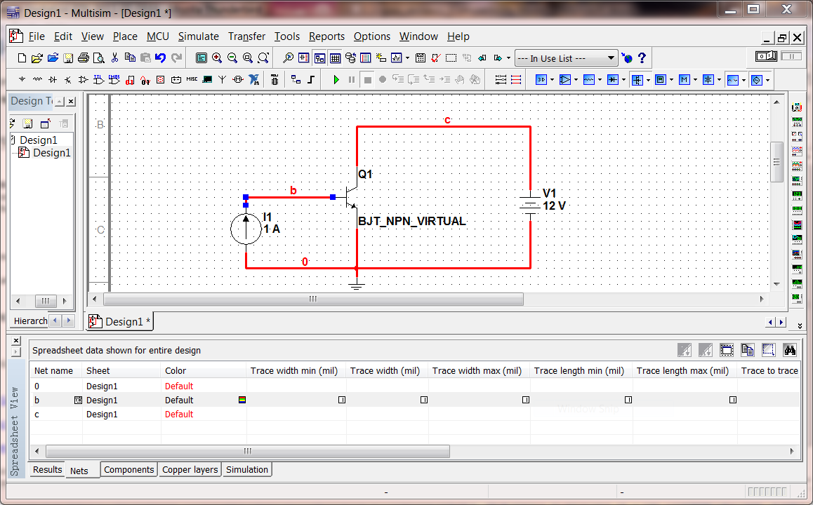
Figure 8: schematic for forced IB output curve simulation
Use Better Net Names
A good circuit simulation practice is to name the circuit nodes (nets) meaningfully. By default, all nodes are named numerically or with some conventions only understood by the program itself. In this case, we want to rename the base node b, and the collector node c. That way, we later can refer to the base voltage by v(b) in expressions so we do not have to try to remember that node 2 is the base node. Later on in CMOS complex logic gates where we can have 20 or 30 nets, it will not be even possible to try to remember the meanings of all nets by number.
The best way to look at all the nets information is through the Nets tab in the Spreadsheet view as shown below:

Figure 9: spreadsheet view of nets
Just click on a net name to make changes, this includes name and color. The color change will be necessary later on. For now, let us just make name changes as follows:
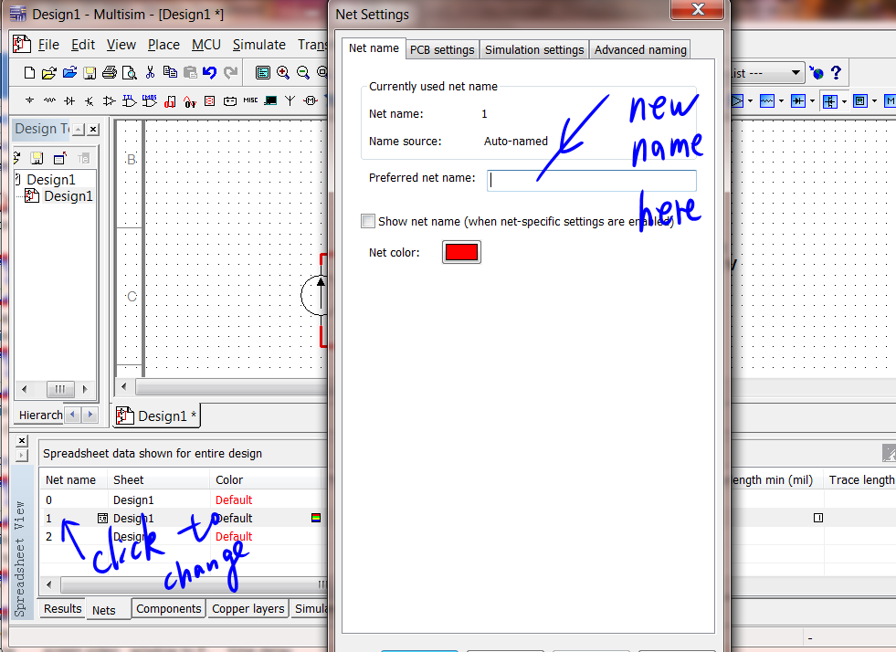
Figure 10: procedures of changing net name
Your schematic now looks like:
Figure 11: schematic with meaningful net names
Change Component Values
Often the default component values need to be changed. For instance, the transistor model parameters need to be changed, which we will discuss in greater detail below. For now, we notice the default value for the current source we use to drive the base is 1A, which is too much for most if not all transistors. Let us change that to 1uA instead to begin with. In general, double clicking a component opens up a window for changing values of its properties. Try this on the base current source:
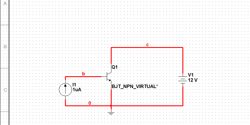
Figure 12: schematic with meaningful net names for 1uA base current
Let us use the default transistor model parameters to proceed with I-V simulation. We will come back to transistor model soon.
General Editing
Much of the usual editing key bindings in other computer programs will work in Multisim, including:
- Ctrl + C for copy
- Ctrol + X for cut
- Ctrl + V for paste
- Delete for delete
- Ctrl + Z for undo
- Ctrl + Y for redo
- Ctrl + S for saving
When multiple instances of an existing component, e.g. ground, or a voltage source, are needed. We can use Copy and Paste.
DC Sweep Analysis
While Multisim provides “instruments” like simulation, which we will cover later, these “instruments” often have limitations. We can have more control or flexibility using Analysis under Simulate. This is close to the Analysis in other SPICE based simulators.
One of the best ways of understanding operation of a transistor or a circuit is to examine how an output of interest responds to an excitation change. For the NPN transistor in question, we want to examine how the output current, in this case, the collector current, changes when the collector-emitter voltage VCE, which is set by V1, sweeps say from 0 to 1V for a given fixed base current of 1uA we set earlier. This can be achieved by sweeping V1, and doing a DC analysis at each V1.
Single Source Sweep
The procedures of V1 (VCE) sweep for a given I1 (IB) are as follows:
From the main menu, select Simulate -> Analyses -> DC Sweep as follows:

Figure 13: finding dc sweep setting
Set the Analysis Parameters tab as follows:
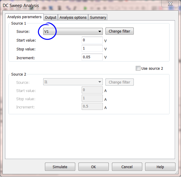
Figure 14: dc sweep setting for Ic-Vce curve simulation under a single Ib input
Click the Output tab, select I(Q1[IC]), click Add to add it to Selected variable for analysis as shown below:
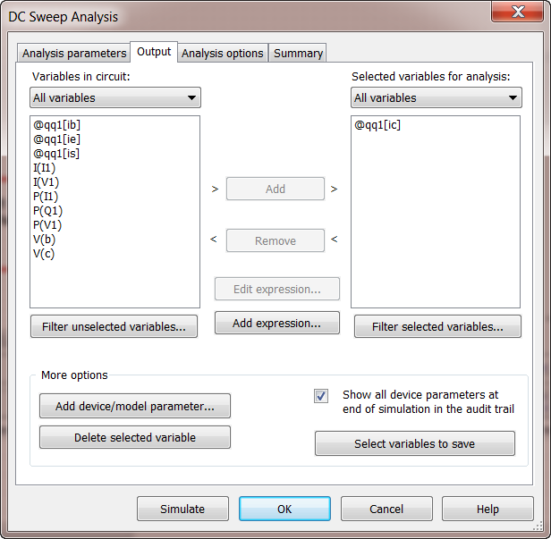
Figure 15: dc sweep output tab setting for Ic-Vce curve simulation
Click Simulate, a grapher window will pop up after simulation is complete, showing the output we selected earlier, IC of Q1:
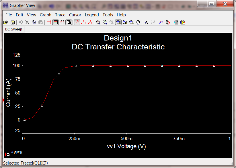
Figure 16: Ic-Vce curve simulated for Ib=1uA
You can change the black background by clicking on the following icon as shown below:
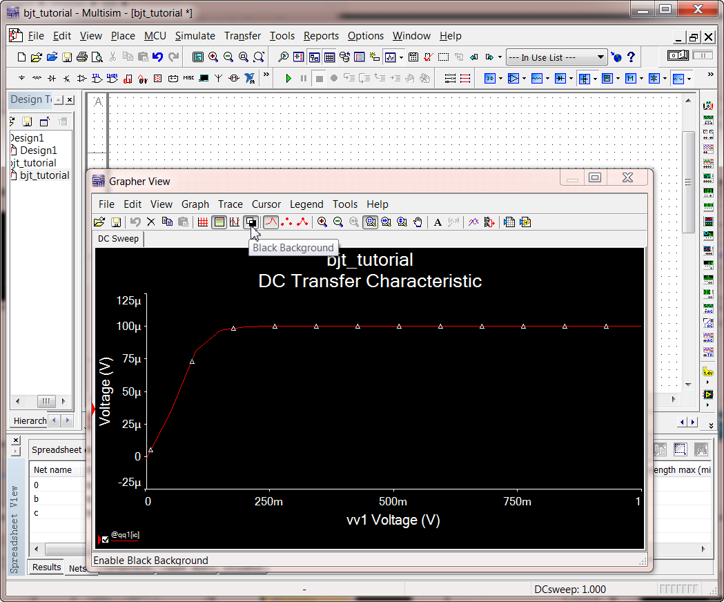
Figure 17: how to change background of a graph
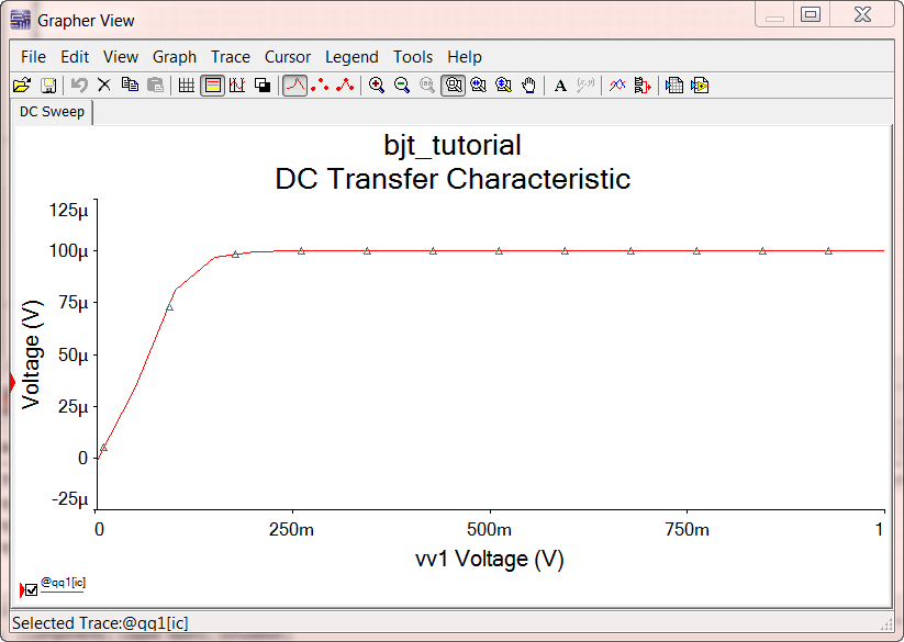
Figure 18: Ic-Vce curve simulated for Ib=1uA with white background
Practice
Plot out VBE and VBC on another graph. Note that emitter is grounded. You will need to use expressions to calculate VBC.
Solution
In Grapher, select from menu, Graph -> Add traces from Latest Simulation Results. A new window pops up. Check To new graph. Add expressions. Your result should look like:

Figure 19: Vbe and Vbc, two junction biases as a function of VCE for Ib=1uA
In this case, having meaningful net names greatly simplifies construction of expressions.
Nested Two Level Sweep
We have obtained a graph of IC vs VCE for a given IB. Next, we would like to know how this curve changes as base current change. What we need to do is to repeat the above DC sweep of V1 for different values of I1 which controls IB.
To achieve this, just go back to the Analysis parameters tab, and check use source 2. Then set the start, stop and increment of the 2nd source, I1 in this case, as shown below:

Figure 20: how to make nested two level DC sweep, IC-VCE for multiple IB as example
The result is a family of IC-VCE curves for the specified base currents:
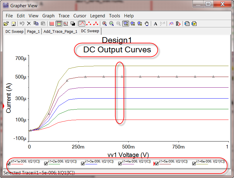
Figure 21: IC-VCE output curves for multiple IB
Note
The red rectangles are added, not from the grapher.
The legends at the bottom indicate values of the 2nd source, in this case, I1 or IB.
Tab name and title can both be changed. You can zoom vertically, horizontally using the zooming tools.
Device Modeling
Why Modeling
There is no question that computer simulations using SPICE like programs such as Multisim are absolutely necessary. The accuracy of circuit simulation, however, is only as good as the accuracy of the device models used internally to describe device electrical characteristics.
The biggest pitfall of circuit simulation is lack of necessary attention to device modeling. Far too often, students and engineers simply assume the models they have downloaded from the Internet or obtained by other means are correct for the devices they are using to build circuits, meaning the models can faithfully reproduce measured electrical characteristics, at least for the biasing condition and frequency of operation in question. Sadly, in most cases, such models are NOT carefully calibrated against measured electrical characteristics.
Extracting or sometimes adjusting parameters of a device model to match measurement is essential. Once we have a calibrated device model, our circuit simulation results will be pretty accurate. One of my research areas is device modeling, which includes not only extracting model parameters to match measured data, but also developing physics based new models when existing models simply fail to work, no matter how parameters are extracted. My most recent project on device modeling is to successfully develop new transistor models to enable integrated circuit design over the wide temperature range from 43K to 393K. The models were used to design integrated electronics that can operate in space as is without warm boxes.
So what if I do not have a good model? Likely the simulation result is just garbage. Many people call this garbage in garbage out.
In our lecture I have made an effort in explaining the solid-state physics basis of bipolar transistor and developing the essential I-V equations that are at the heart of bipolar transistor models used in all circuit simulators. You are equipped with the knowledge to understand the essential transistor model equations and list of parameters.
You might wonder how can a generic virtual transistor model represent any transistor? I wondered as a sophomore student. The answer is it cannot possibly do so. The so-called real component transistors often use the same transistor model equations, but with different model parameters extracted for that transistor. However, the general paractice of serious designers is to still calibrate its model parameters against measurement. If calibration is not possible, at least we want to find out if the simulation matches measurement for characteristics of interest.
As a first step towards successful circuit simulation, we want to know how to find out what device model is used in our simulator, and how to modify model parameters. We can for instance, measure transistor’s forward beta BF and reverse beta BR, saturation current IS, and put them into Multisim, rather than relying on the generic default values for bipolar transistor.
Editing Model Parameter in Multisim
To edit model parameters of a transistor,
double click the transistor
click Edit model
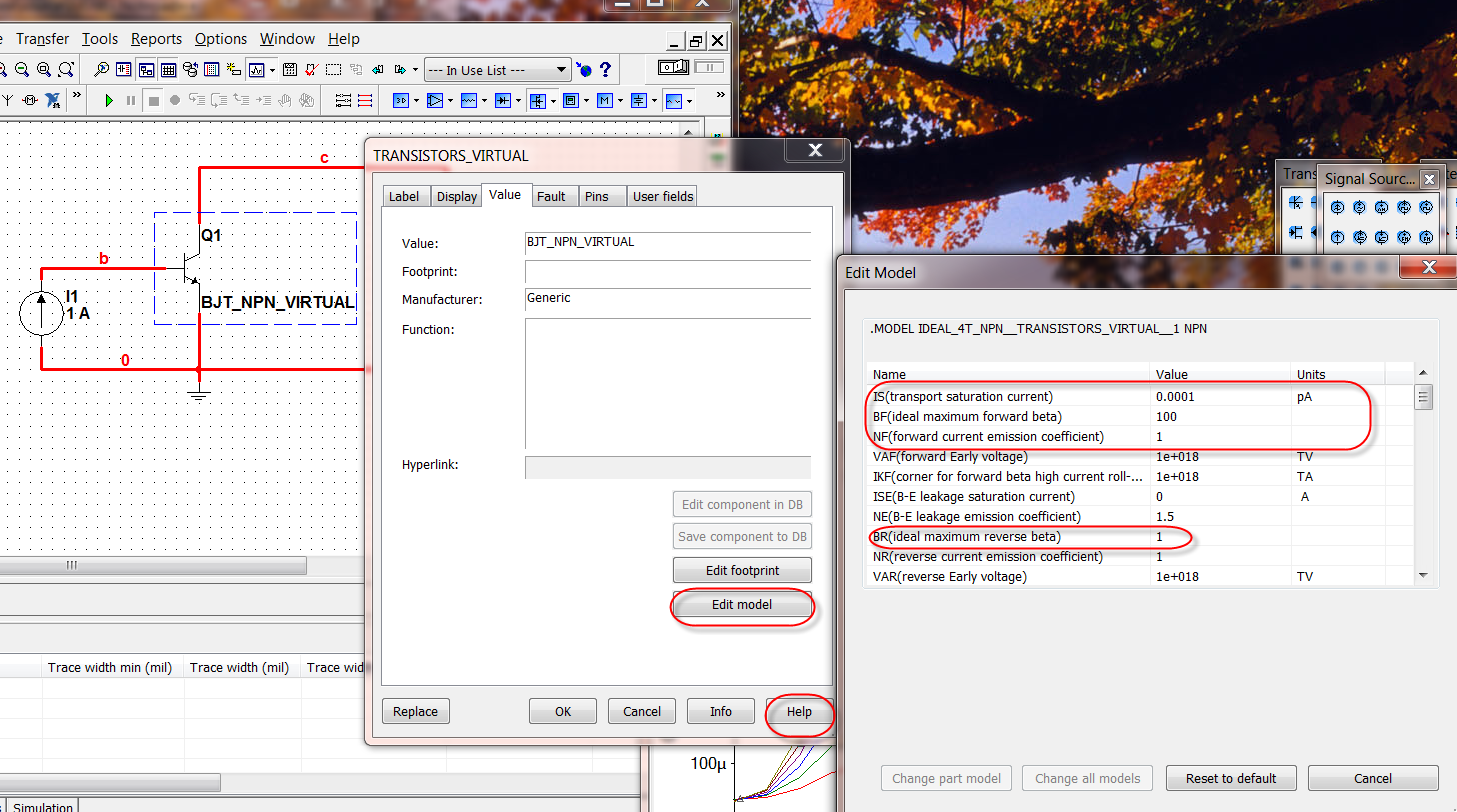
Figure 22: how to edit transistor model parameters
The first entry in the model parameter table is IS, the saturation current. The second entry is BF, forward beta. The third entry is NF, foward ideality factor, incorrectly called “forward current emission coefficient”. You can also see the reverse beta BR and reverse ideality factor NR.
As you can see, a transistor model has many more parameters than what we use in hand analysis.
You can edit a model parameter’s value here.
You may use several different transistors in the same design. They will need to have different model parameters. It is important to know what parameters each transistor use.
The most convenient way of examining the models and/or model parameters each transistor uses is to view the netlist.
On main menu, select view -> Spice Netlist Viewer. A window of the netlist pops up. You can copy the netlist to clipboard. The netlist for the above circuit is shown below:
** bjt_tutorial **
*
* NI Multisim to SPICE Netlist Export
* Generated by: GuofuNiu
* Sun, Jun 05, 2011 23:08:39
*

*## Multisim Component V1 ##*
vV1 c 0 dc 12 ac 0 0
+           distof1 0 0
+           distof2 0 0

*## Multisim Component I1 ##*
iI1 0 b dc 1e-006 ac 0 0
+           distof1 0 0
+           distof2 0 0

*## Multisim Component Q1 ##*
qQ1 c b 0 IDEAL_4T_NPN__TRANSISTORS_VIRTUAL__1__1


.MODEL IDEAL_4T_NPN__TRANSISTORS_VIRTUAL__1__1 NPN
+  IS=1e-015 VAF=1e+030 IKF=1e+030 BR=10 VAR=1e+030 IKR=1e+030 IRB=1e+030
+  RBM=0 VTF=1e+030
You may notice that the parameter list is not as long as in the model parameter table we saw earlier. This is simply because only parameters with values different from the default values need to be stated. If a parameter is not shown, it takes on the default value.
Homework Problems and Solutions
The best way to learn is to experiment yourself. Below are some homework problems. You will need to use expression.
Homework Problems
Use Virtual NPN, edit model such that IS=1e-15, BF=100, BR=5. Read (and follow) the new tutorial first. Complete the following simulations and plotting tasks. You need to create a circuit schematic that is designed to complete the required simulations first. You can also read mistakes made by past students given below at the end of this tutorial.
Simulate IC and IB as a function of VBE when VBC is set to zero. Range of VBE is from 0.2 to 1.0 V in step of 0.02V. Use log scale for y-axis (current axis). This type of plot is known as Gummel Plot widely used in experimentally characterizing transistors.
Your circuit schematic should look like this for Gummel plot simulation:
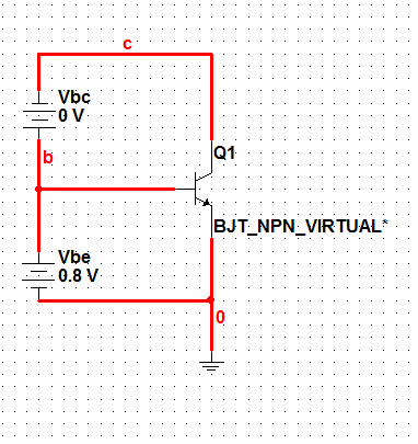
Figure 23: schematic for simulating Gummel characteristics
Using the simulation results of the previous step, plot out beta as a function of VBE, defined as the ratio of IC to IB using expressions.
Comment on if the beta simulated is consistent with BF value you put in.
Simulate IC as a function of VCE for several VBE values. VBE is from 0.7 to 0.75V, in step of 0.01V. VCE is from 0 to 3.5V, in step of 0.1V. Note VCE sweep is primary.
Indicate the forward bias region and saturation region on the IC-VCE output plot. Your circuit should look like this:

Figure 24: schematic for simulating forced-VBE (or voltage drive) output characteristics
Your output should look like:
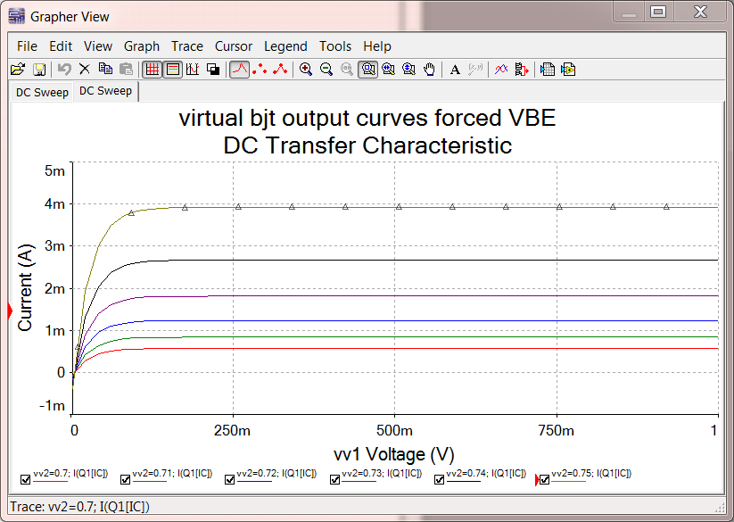
Figure 25: sample plots of forced-VBE (or voltage drive) output characteristics
You will need to use VBE as source 2. This type of plot is known as forced VBE output plot.
Simulate IC as a function of VCE for various IB values. This is known as forced IB output characteristics. IB is from 0.1uA to 1uA, in step of 0.1uA. VCE is from 0 to 3.5V. Indicate the forward bias region and saturation region on the IC-VCE plot.
Repeat the forced-VBE output plot simulation using a different reverse beta, BR=1.
Compare the output graph with that of BR=10 obtained earlier.
(Extra 10 point credit). Explain the difference between the BR=10 and BR=1 results.
Need screen shots of:
- schematic
- model parameter list, you can attach the netlist for this
- analysis parameter settings
- all simulation result plots with proper labels
Mistakes and Solutions
Below are mistakes I have seen in helping students debug Multisim simulation.
Incorrect circuit configuration. For instance, VCB is placed between C and E.
Use default values for components. For instance, when you add a voltage source and use it for VCB, the default 12V is too high, and breaks down the transistor.
Plot out currents, IB and IC, and ratio of IC/IB all together. In general, this does not make sense. Use new graph as shown above for VBE and VBC plotting in forced-IB output circuit.
An expression, e.g. beta = ic/ib, must be created. An example of how to do this is:
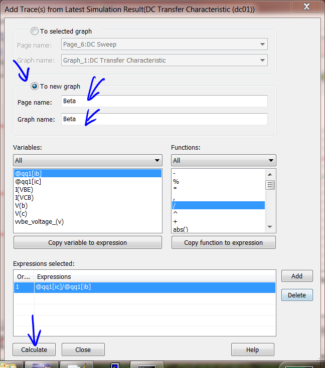
Figure 26: how to create a new trace using expressions after a simulation
Use default labels. Default labels are often voltage even if you are plotting currents. Change them manually to avoid confusion.
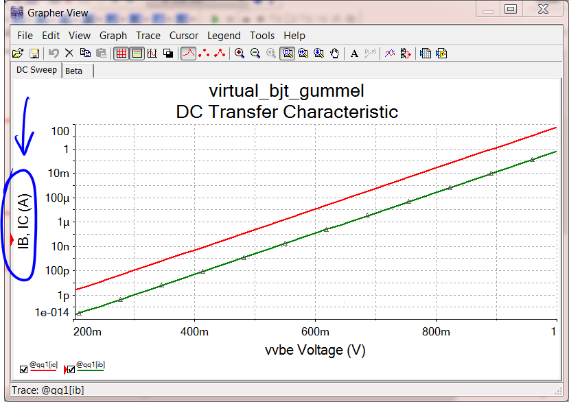
Figure 27: forward mode Gummel plot, i.e. IC and IB versus VBE. VBC=0
Your beta (IC/IB) should look like htis:
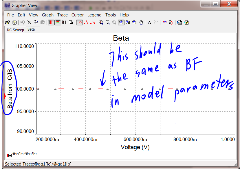
Figure 28: how to create and add a new trace using expressions after a simulation