8. Gate Length Scaling on Transistor Electrical Performance
8.1. Objectives
The objectives for this project are:
- use swb to manage large complex experiments
- understand impact of gate length on Vth, SS, Ion, Ioff, DIBL etc.
8.2. Required Programs
- sde
- sdevice
- tecplot_sv
- inspect
- swb
- nmos_physics.gzp (25 MB - so large) from /scratch folder
8.3. Get Files
To get the swb project file, log on to niu003, run
cd
/scratch/getfiles.sh
Then, in a terminal, run
swb
Load in the nmos_physics.gzp, and extract all into a folder of your choice.
8.4. Gate Length Impact
8.4.1. Threshold Voltage Roll-off and Reverse Short Channel Effect (RSCE)
As gate length scales down from 1um to 30nm, run all the Id-Vg simulations, then run the very last “Roll-off” node, only the last is meaningful, it is a trick to make plots of extracted variables versus lgate.
You can always open up a spreadsheet - move your mouse over one of the icon that says spreadsheet if you wish to do so.
Follow on-screen instruction. The 2nd screen plots out the current defined threshold voltage at low Vd and high Vd (50mV and 1.2V), vti, and DIBL, defined as the amount of vti change per voltage change in Vd, as a function of lgate:
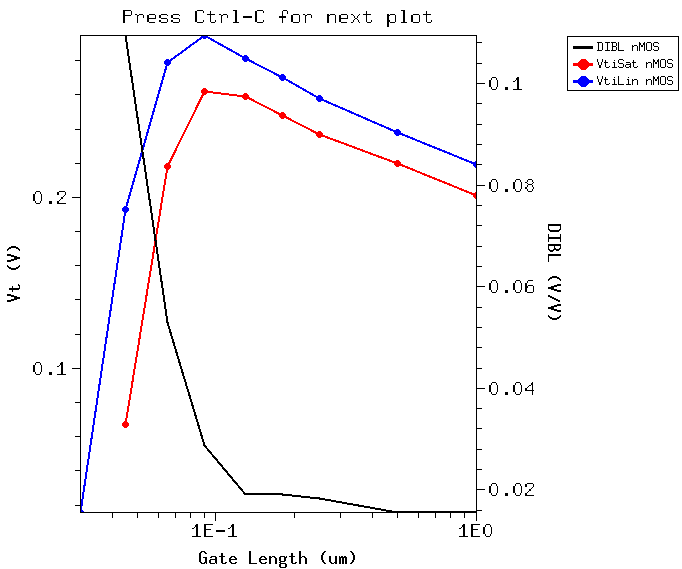
Figure 1: Vti linear, Vti saturation and DIBL vs lgate from 30nm to 1um.
We see clearly with decreasing lgate, the Vt’s increases first, due to the rising average channel doping, because of the halo doping, but eventually decreases with further scaling down of lgate, due to the increasing impact of the drain to channel junction on surface potential with decreasing gate length.
You can examine the tdr files as necessary for deeper insights.
I suggest that you plot out the surface doping or near surface doping along the channel. It is a 2D effect, yes. But a 1D plot along the channel at the surface will allow you to better see the numbers, and how the doping along the channel changes as you scale down lgate.
Once you are in tecplot_sv, and have made the cuts, it is easy to quickly inspect other variables, like potential and n. Save some plots, you should then be able to link what happens microscopically inside your device with its electrical characteristics at the terminals.
Such insights will also be very useful later on in our next semester’s Elec7710 class on more advanced topics, including device design and compact modeling.
You can also change halo doping level or make it very low compared to substrate doping, and then see how your results change.
Below are more plots from running the Roll-off node, I am going to leave analysis to you for now.
8.4.2. Off State Current Ioff
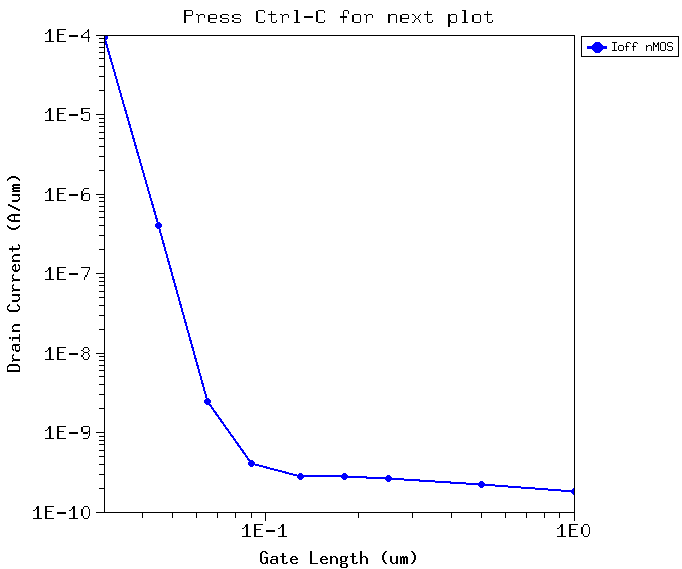
Figure 2: Ioff vs lgate from 30nm to 1um.
8.4.3. On State Currents and Ion
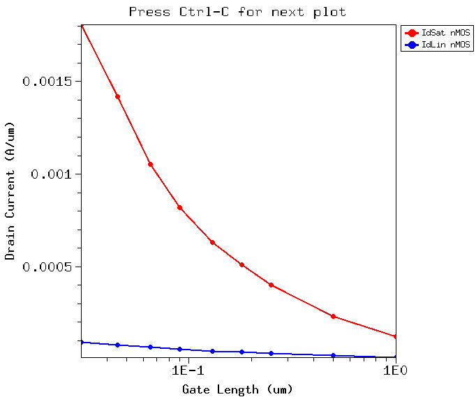
Figure 3: I(vg=vdd) vs lgate from 30nm to 1um. I(vg=vdd, vd=vdd) is called Ion.
8.4.4. Ioff vs Ion
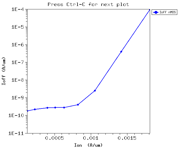
Figure 4: Ioff vs Ion from 30nm to 1um. I(vg=vdd, vd=vdd) is called Ion.
8.4.5. Gm vs lgate
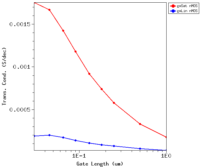
Figure 5: Gm in linear and saturation vs lgate from 30nm to 1um.
8.5. Operating swb
You can refer to the swb user guide located in that same folder as sdevice, swb_ug.pdf, for more information on using swb.
For your class project of IdVg_lin simulation, you can modify the Vd used in the Vg sweep. There are a few ways to do this. L The simplest way is to just modify the value of the parameter Vdlin from 0.05V to say 0.5V.
To modify the value of Vdlin, select it. The right click, Edit values as shown below:

Figure 6: Editing parameter value.
Remember to preprocess and then run the IdVg_lin swb nodes involved. Hole control to select multiple nodes.
Then you should preprocess and run the inspect nodes as well.
Finally, update the variables in swb manually if it has not been set to auto update.