4. MOSFET Id-Vd Output Curves Simulation and Probing of Internal Physics
4.1. Objectives
- perform Id-Vd simulation
- learn how to save and load solutions for better convergence
- examine internal physics, particularly at the surface
- better understand what happens beyond “saturation”
4.2. Required Programs
- sde
- sdevice
- tecplot_sv
- inspect
4.3. Overview
See lecture notes on 3-terminal and 4-terminal MOS devices.
4.4. Files You Need
Download the files from our class sites. Use the large file which has more up to date contents. If you home directory is small, download it to a PC first and pick files you need. You can take out the *.cmd files and *.par files, and run them to generate all other files you need.
Once you download the file, go to file browser, then right click Extract here.
Typically you should put it under your home folder for ease of access, then do extraction.
4.5. Meshing
To generate the mesh, first edit structural parameters in the halomosfet_sde.cmd file. In a terminal, cd to the source file folder, just run
gedit halomosfet_sde.cmd&
For now, you do not have to change anything. You should find the script is written such that you can modify structural parameters easily. After editing, save the file. You do not have to close the editor as it is running in background.
Next, run
sde -l halomosfet_sde.cmd
You will see sde working to generate the MOSFET mesh. You can then close the sde program. At this point, you can also use tecplot_sv to inspect the structure produced.
4.5.1. Halo Doping
One important feature to notice is the placement of halo doping, a pocket of relatively high concentration p-type dopants near the source and drain. This is important to limit the depletion thickness of the lateral n+ source/drain to p-channel junction, to reduce electrostatic coupling between the source and drain.
Inside tecplot_sv, do a 1D cut of the y-axis, specify a y location at the surface, then observe the plot. Due to numerical issues with tecplot_sv, you likely will run into trouble with not getting the entire distance along the x-axis plotted.
So I suggest that you use either cut-along-boundary, or simply just give a point right below surface, e.g. y = 0.001. The doping variation along the cut line should look like:
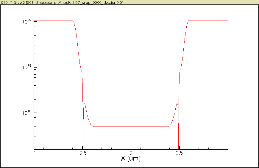
Figure 1: Doping variation along MOSFET channel at the surface showing halo doping.
4.6. Simulating
Examine the idvd_des.cmd file first. As we explained in class, for better convergence, we do a Vg sweep at zero Vd first, save them. Then we load each Vg with zero Vd solution, and ramp up Vd. In this example, the source and body are both at zero, so you do not see body bias effect at the source end. This can be easily changed by modifying the body bias.
Then run
sdevice idvd_des.cmd
You should see reporting of solution process.
4.7. I-V Plotting and Unit of Current
Examine idvd_ins.cmd file first. You do not have to completely understand it, but just a quick look will give you some useful idea about what it does. You may modify it for your purpose. You are not required to write such programs.
Then, run
inspect -f idvd_ins.cmd
You should see a nice Id-Vd plot as follows:
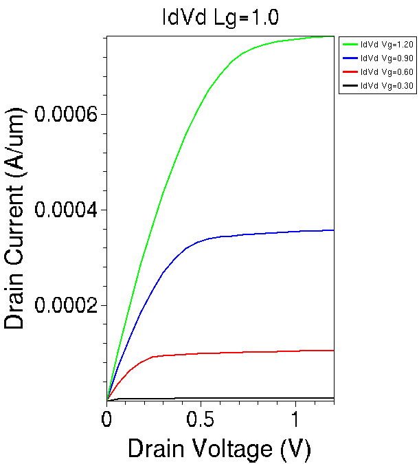
Figure 2: Simulated Id-Vd output family of curves.
You might wonder why the unit of current is A/um, not A. Good question indeed. This is a 2D simulation, we never gave the simulator any information on the dimension along the 3rd dimension. Real objects are 3D of course.
By default, the simulator assumes a 1um width in the 3rd dimension. In our MOSFET case, it means the default channel width is 1um.
This of course can be changed. We will get to that later, or you can look up the manually to quickly find out how to change this.
Note
Think about what the unit of terminal resistance should be for a 2-D simulation.
4.8. Probing Internal Physics for Understanding
To probe internal physics, in a terminal, run
tecplot_sv
From reading the *des.cmd files, you should know what all the .tdr files are.
Make a y-cut at y=0.001 (0 strictly speaking, see above for why), the surface of Si. We can plot out Ec, Ev, electrostatic potential, Efn, Efp, phi_fn, phi_fp etc. along the cut.
4.8.1. High Vg
Recall the names of the highest Vg .tdr files. Load them in tecplot_sv as follows:

Figure 3: Loading high Vg (1.2V) tdr files for different Vd.
Remember to Add the files selected. Then OK.
Then go to slicer -> Orthogonal Cut. Select Y as normal direction. Deselect Cut at mouse position. Set first cut at to desired value, e.g. 0.001 here. Then create cut.

Figure 4: Making y-cut at desired location.
Click on the rearrange frames icon in the tool bar in the top left area of your tecplot window to focus on the cut plot. Disable the legends by clicking the legends on /off icon. Too busy a plot with them.
By default you see the doping. Now you can select other quantities of interest. Let us look at a few of them:
4.8.1.1. Potential and Field

Figure 5: Surface potential along channel. Vg=1.2V. Vd from 0 to 1.2V.
As Vg is high, well over threshold voltage, with a Vds, current flows, potential drop varies along the channel. The amount of variation is equal to Vds (Vd here as Vs is zero).
At Vd=0.2V, 0.4V, 0.6V and 0.8V, all the Vds drops over the channel region. We can see an increase of lateral field with increasing Vd, as expected.
At Vd=1.0V and 1.2V, the potential in the channel barely changes, and stays about the same as at Vd=0.8V.
4.8.1.2. Hot Electrons and Reliability
The extra Vd drops in a vary narrow region near the drain, a sharp change of potential in a narrow region means high field. So keep this in mind, lateral field is strongest near the drain after the so-called pinch off occurs. This also leads to hot electrons, which can hit the oxide/Si interface, causing damages over time. This is one of the important considerations for long term reliability of transistors and CMOS ICs in general.
4.8.1.3. Conduction Band Energy, Journey of Electron

Figure 6: Ec along channel. Vg=1.2V. Vd from 0 to 1.2V.
This pretty much correspond to the surface potential plots. Electrons in the N+ source move from the source to the channel, and drift down hill towards thee drain.
Note the sharp band bending near the drain after Vd is above 0.8V.
The Ec in the active channel region no longer changes much after saturation.
4.8.1.4. Channel Length Modulation
The point at which we see rapid change of Ec moves towards the source a little bit wiht increasing Vd. This is known as channel length modulation. Electrical channel length decreases a bit with further increase of Vd after saturation, causing the drain current to increase slightly. In circuits, this will cause some output conductance, or a finite amount of output resistance, limiting the so-called open-loop voltage gain of a transistor amplifier.
4.8.1.5. eQuasiFermiPotential

Figure 7: eQuasiFermiPotential along channel. Vg=1.2V. Vd from 0 to 1.2V.
Recall that at strong inversion, which is the case for the whole channel except for near the drain, electron quasi Fermi potential follows the electronstatic potential (surface potential roughtly is Vcb + a constant).
We see this behavior in this plot.
4.8.1.6. eGradQuasiFermiPotential

Figure 8: Gradient of eQuasiFermiPotential along channel. Vg=1.2V. Vd from 0 to 1.2V.
Gradient of eQuasiFermiPotential is driving force of current. We see this clearly in the plot.
4.8.1.7. eQuasiFermiEnergy

Figure 9: eQuasiFermiEnergy along channel. Vg=1.2V. Vd from 0 to 1.2V.
This is very much the opposite of eQuasiFermiPotential. Recall that Vcb is equal to Vds at the drain.
4.8.1.8. eDensity

Figure 10: eDensity along channel. Log scale. Vg=1.2V. Vd from 0 to 1.2V.
This is a plot you really would like to not use the y=0.001 cut. I recommend using the cut-along-boundary function. Reason? Even a 0.001um separation can make large difference in eDensity. This, however, cannot be done automatically without using mouse to position the start and end points of the boundary. Also I have not found a way to repeat the cuts on all biases loaded. Below is a cut-along-boundary result for the Vg=1.2V and Vd=1.2V case:

Figure 11: eDensity along channel obtained using cut-along-boundary. Log scale. Vg=1.2V. Vd from 0 to 1.2V.
Still we see a clear picture of how electron density varies along the channel, that is, it decreases from source to drain, as we well expect from our 3-terminal MOS theory.
The amount of decrease is dependent on Vd which sets Vcb. From source to drain, gate voltage is the same, but Vcb increases from 0 to Vds in this case. Electron density thus decreases from source to drain.

Figure 12: eDensity along channel. Linear scale. Vg=1.2V. Vd from 0 to 1.2V.
This is a linear scale eDensity plot.
4.8.1.9. Electron Velocity and Pinch-off

Figure 13: Electron velocity along channel. Linear scale. Vg=1.2V. Vd from 0 to 1.2V.
Note that we are using a highly simplified mobility model, with no velocity saturation. So you see very high velocity, particularly near the drain at high Vd.
Again, we should understand that electron density does not go to zero anywhere along the channel. If it does, or it does pinch off completely at any point, it would be an open circuit, and block current flow.
The so-called pinch-off is just a crude way of saying surface is no longer in strong inversion. Even in weak inversion there are finite electrons. A small amount of electrons can travel at very high velocity to still support a large current.
Again, note the high velocity and hence high kinetic energy of electrons near the drain, which can hit the oxide and create damages of the gate oxide/Si interface.
4.9. Homework
Pick one of the 3 problems below that is assigned to you, and complete it before Oct 14 class time. Bring your plots / files on a flash drive for sharing. You can work in groups if you wish, but each person needs to produce plots and analysis by himself/herself.
- (Olive, George, Wei-chuang, Jingshan) Follow the notes above, and repeat these plots and write down analysis as well as observations for Vg=0V and 0.6V. Associate the plots with your understanding and theory in any way you can. Save each plot as a .png file as well. Name each plot meaningfully.
- (Zhenzhen, Kun, Fang, Ruocan) Repeat these plots for the .tdr files generated from running idvglin_des.cmd and write down analysis.
- (David, Suraj, Pingye, Zhen) Repeat these plots for the .tdr files generated from running idvgsat_des.cmd and write down analysis.
Of course, you can choose to work on all of them as well.