2. Semiconductor Fundamentals Illustration with TCAD
2.1. Objectives
- Understand quantitatively how fundamental material parameters vary in semiconductor, e.g. band gap, electron affinity, dielectric constant
- Understand relationships between various potentials and energies important for understanding device operation
- Understand how biasing affects various potentials and energies at device terminals / ohmic contacts
- Introduce essential concepts of surface charge modulation
2.2. Required Programs
- tecplot_sv 2010 version (2008 version may work as I use latest features of Sentaurus, I did not check this. The .cmd files did not work with sdevice 2008). As of 8/21/2011, there is issue with running tecplot_sv on the engineering Linux workstations. I have reported the problem and hopefully the issue will be resolved soon. I will then supply you with the necessary files and give you a live tutorial on how to inspect TCAD simulation outputs. To keep it manageable, we will focus on using existing codes provided so that you can use TCAD to understand devices without having to spend a lot of time putting together working TCAD input decks or coding.
2.3. Overview
There have been many good books on semiconductors and devices you can refer to for theories. In this lecture, we will look at a concrete numerical example using TCAD, with a 1D cut done on a 2D MOSFET structure.
By design, we will simulate the polysilicon gate as polysilicon, rather than a piece of ideal metal gate with an artificially adjusted work function. This is a much better approximation to reality, and allows the important polysilicon gate depletion effect to be correctly accounted for.
This choice has a unique advantage of allowing easy visualization of effects of bias on quasi-Fermi potential energies and potentials at device terminals. The easiness is a result of zero current flowing vertical through the MOS structure. The quasi-Fermi potentials or energies are therefore spatially constant in the polysilicon gate, and thus easy to visualize. For similar reasons, we can see the impact of bias on potentials clearly this way.
Let us first look at structure and material parameters.
2.4. Device Structure
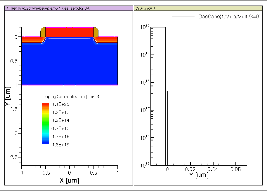
Figure 1: 2D MOSFET simulated and 1D cut at x=0 showing the N+ poly gate doping level and p-substrate doping level.
2.5. Material Parameters
2.5.1. band gap Narrowing (BGN)
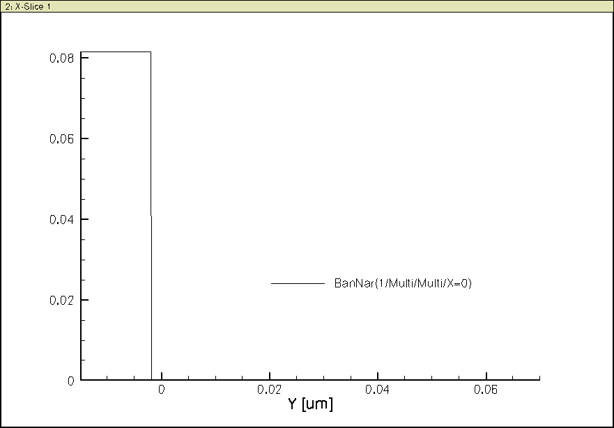
Figure 2: BGN is observed in N+ polysilicon gate because of heavy doping
2.5.2. Effective band gap
band gap in the gate oxide is much larger than in Si.
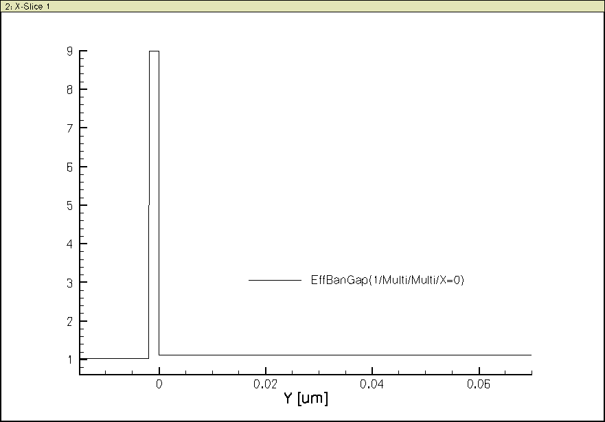
Figure 3: Effective band gap is smaller in N+ polysilicon gate because of heavy doping induced band gap Narrowing (BGN).
2.5.3. Electron affinity
The amount of energy it takes to free an electron at the bottom of the conduction band, i.e. the Ec level, is called electron affinity. You can also consider this to be the difference between the so-called vacuum energy level and Ec.
Electron affinity can be used to determine the Ec alignment or offset between two different material regions, e.g. between the gate oxide and N+ polysilicon gate, between the gate oxide and the silicon substrate.
Similarly, we can determine Ev alignment between two material. We need to account for the band gap difference in addition to electron affinity difference.
Electron affinity and band gap differences will also be used to determine band alignments at heterojunction interfaces as well. So keep this in mind.
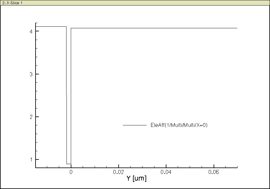
Figure 4: Electron affinity.
2.6. Zero Bias
2.6.1. Electrostatic Potential
Consider zero bias at all terminals. There is still built-in potential. The most convenient reference is a piece of intrinsic semiconductor in TCAD. Hand analysis in textbooks, however, uses different reference. This is very important to note so that you know precisely how to associate simulation results with first order theories in textbooks.

Figure 5: Electrostatic potential. Note reference is the potential of an intrinsic semiconductor under zero applied bias.
For example, in the p-body, potential is -0.45 eV, as its potential is lower than that of an intrinsic piece by 0.45 eV.
2.6.2. Band Diagrams with Vacuum Level
The quasi Fermi potentials at all contacts are simply equal to the applied voltages. Since we are applying zero voltages at both gate and body, the quasi Fermi potentials are zero.
Quasi Fermi energy is simply the inverse of quasi Fermi potential, if you use eV for energy, and V for potential.
There is built-in potential between the N+ polysilicon gate and the p-body. Potential is higher in the N+ poly gate, lower in the p-body.
Therefore, the Ec at the gate is lower than the Ec deep in the body.
I have also calculated the vacuum energy level, which is simply equal to Ec + affinity. The vacuum energy level is no longer spatially constant, because of the built-in electric field. The gradients of Ec, Evac, Ev are all the same, determined by electric field.
Electron affinity and band gap differences will also be used to determine band alignments at heterojunction interfaces as well. So keep this in mind.
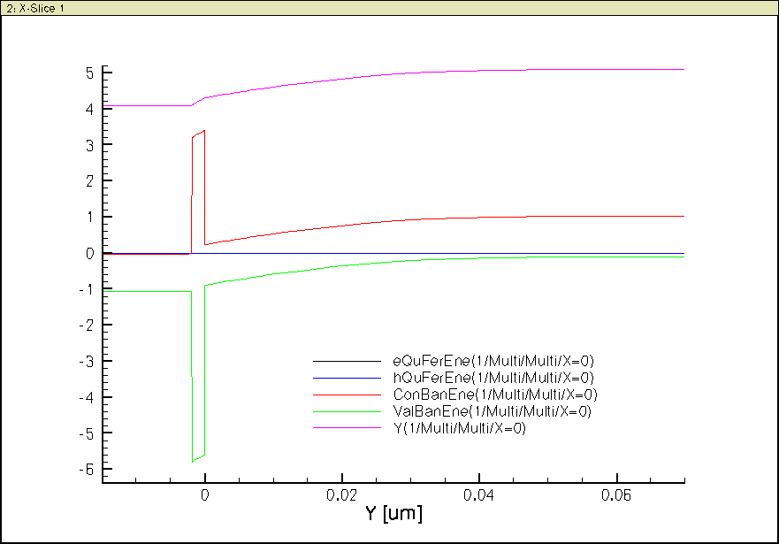
Figure 6: Band diagram with Evac, the vacuum energy level.
2.6.3. Band Diagrams with Intrinsic Fermi Level
Often we do not draw the vacuum energy level, despite its great importance described above. We draw only Ec, Ev, Efn, and Efp.
That is enough information as we know n, p, and electric field (from gradient of band edges).
However, often we also draw the intrinsic Fermi level, or Ei, particularly in hand analysis. The reason is simple. It allows easy visualization of whether a region is n-type or p-type.
In regions where Efn = Efp = Ef, if Ef > Ei, it is n-type. If Ef < Ei, it is p-type.
Below is a band diagram showing Ei:
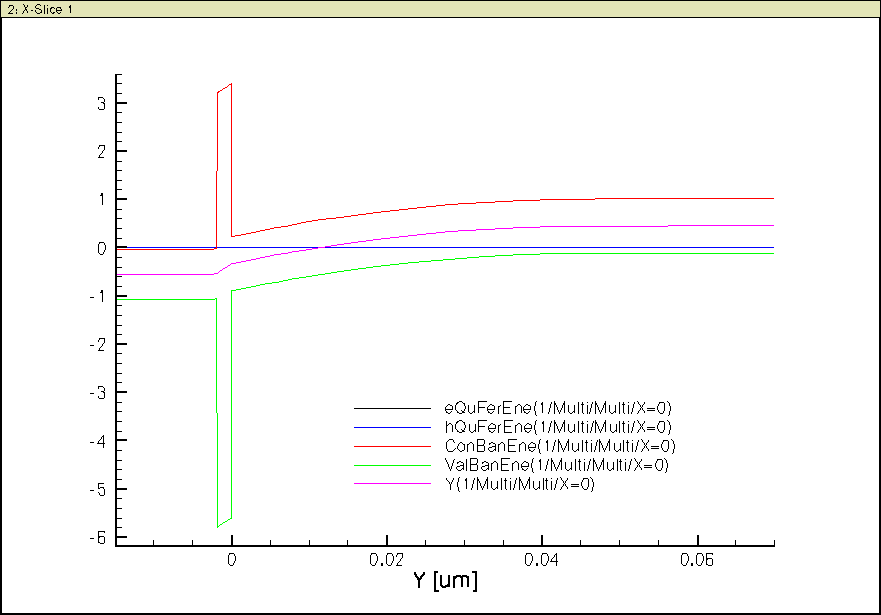
Figure 7: Band diagram with Ei, the intrinsic Fermi level.
Because of the doping difference between N+ poly gate and p-body, there is band bending at the silicon surface. You can easily picture how electron concentration n and hole concentration p vary from this band diagram.
Sketch that yourself, then compare with the following plots:
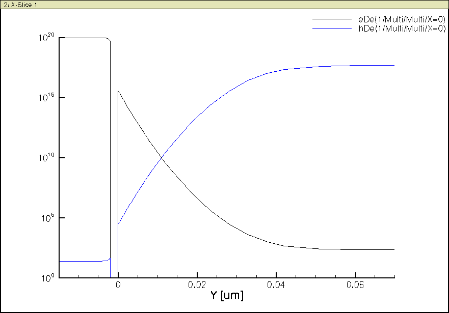
Figure 8: n and p at zero bias.
Observe how n increases towards the gate oxide/Si interface and p decreases in the process. The pn product is kept constant.
Can you explain why the pn product in the N+ poly gate is larger than in the Si body?
2.7. Gate Bias Dependences
Recall from Elec6700 that at ohmic contacts, no deviation from equilibrium is allowed. This means that both n and p values are kept at their equilibrium values, determined by doping at the contacts.
Also recall that Efn and Efp must then be equal at the contact points.
In the MOS structure, there is no gate current for ideal gate oxide. Therefore, Efp and Efn are spatially constant in the N+ poly gate.
The Ef difference between the gate and the body contact (the contact points only) is set by the applied bias voltage difference.
If we simply set the Ef at the contacts to the applied bias voltage, we can prove that the electrostatic potential at a contact must then be equal to the applied voltage + the built-in potential of that contact with respect to an intrinsic reference. I’ll leave the proof to you. Stop by if you have trouble doing so.
The (quasi) Fermi potentials at the contacts are therefore simply equal to their applied voltage values. Now let us keep the body grounded, i.e. at zero bias, and vary the gate voltage from 0 to 1.2 V in 0.2 V step.
Analytical treatment of the 1D MOS structure will be made in a few lectures. Below we show the internal distribution of physical quantities as a function of gate biases from TCAD. A small Vds of 0.05V is applied while the gate bias increases.
2.7.1. Electrostatic Potential
The electrostatic potential distributions for all gate biases are shown below in figure 9:
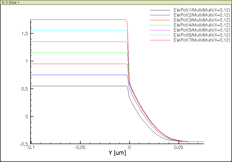
Figure 9: Electrostatic potential for all gate biases.
Observe that for Vgs>=0.4V, the potential in the Si surface region changes very little. Much of the further gate voltage increase is absorbed by the very thin gate oxide, there is also a tiny but noticeable amount of potential drop in the heavily doped N+ poly gate, near the gate/oxide interface.
Why this is the case will become clear once we examine the band diagrams.
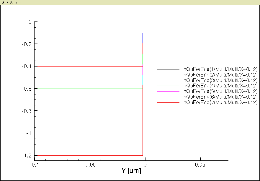
2.7.2. Quasi Fermi Potentials
2.7.2.1. electrons
The electron quasi Fermi potential distribution for all gate biases are shown in figure 10:
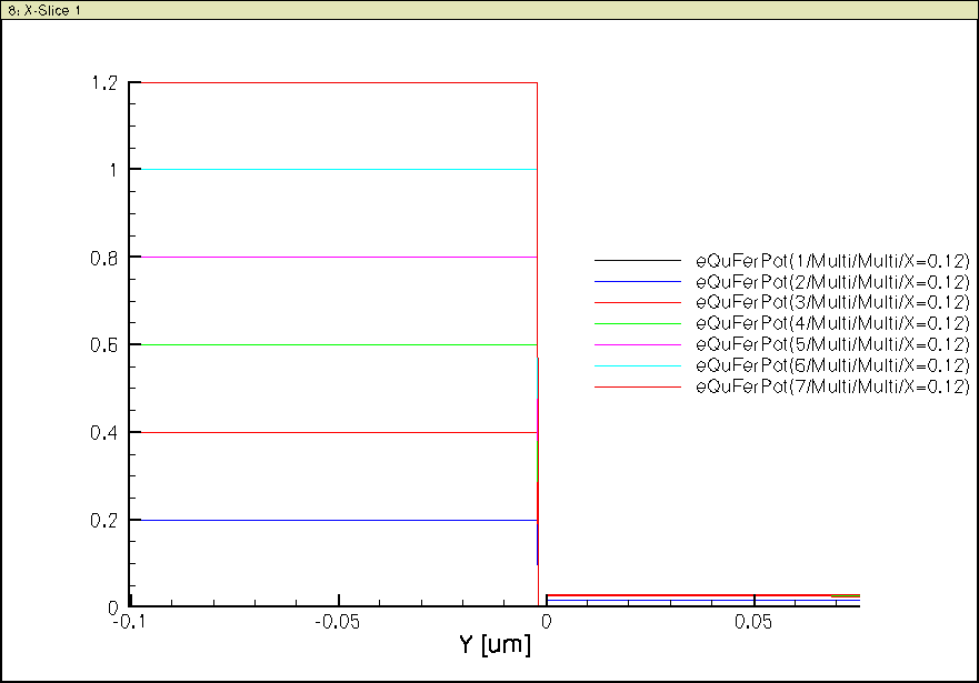
Figure 10: Electron quasi Fermi potential distribution for all gate biases.
Observe that the quasi Fermi potential is equal to zero in the silicon substrate (body), and equal to the gate voltage in the N+ polysilicon gate.
2.7.2.2. holes
The hole quasi Fermi potential distribution for all gate biases are shown in figure 11:
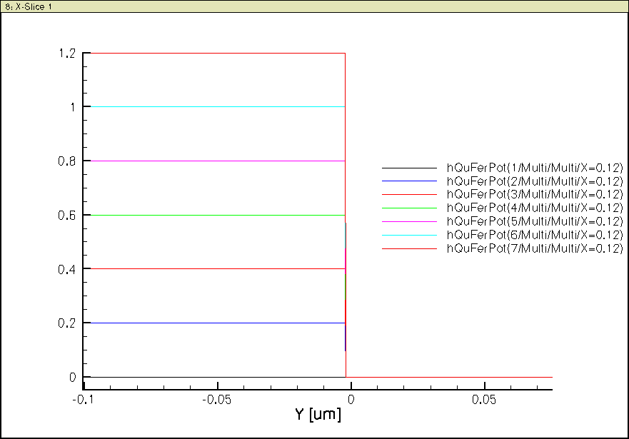
Figure 11: Hole quasi Fermi potential distribution for all gate biases.
Observe that the quasi Fermi potential is equal to zero in the silicon substrate (body), and equal to the gate voltage in the N+ polysilicon gate.
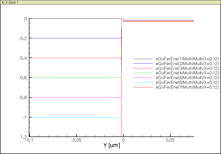
2.7.3. Quasi Fermi Energies
2.7.4. Band Diagrams
Now let us look at the band diagrams for all biases shown below in figure 14:
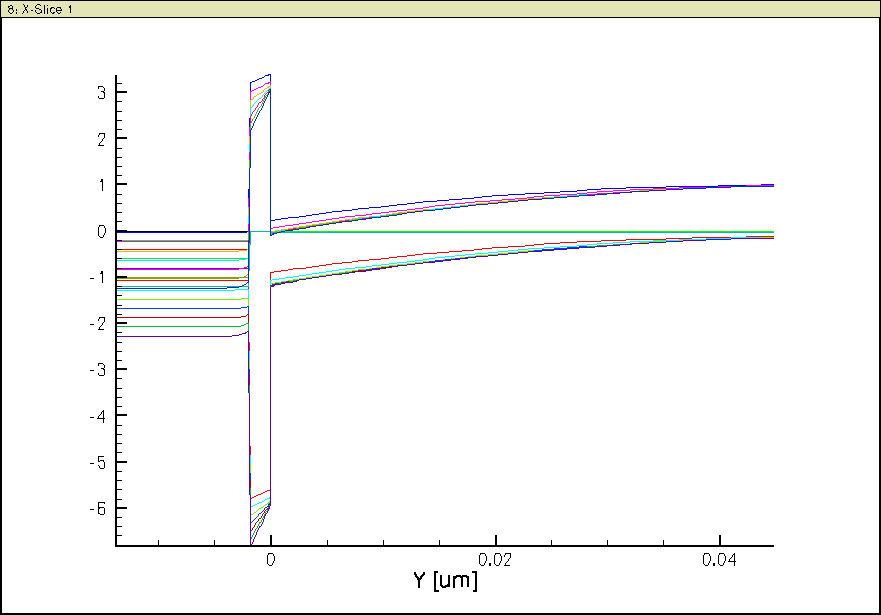
Figure 14: Band diagrams- all bands
The nearly flat curves in the silicon substrate are the quasi Fermi energies of electrons and holes, with a very small separation due to the small 0.05V Vds. For all practical purposes, just view them as spatially constant and equal to 0 eV, the substrate terminal’s applied voltage, or its inverse strictly speaking.
Observe that for Vgs>=0.4V, just a little bit more band bending occurs with further increase of gate voltage. This is because the surface electron density (n) is already very high, any small increase produces enough negative electron charge to shield the vertical gate field. Again, recall the letter n means negative. Much of the further voltage drop occurs now in the gate oxide, as indicated by the increasing slope of the band bending inside the thin gate oxide.
A plot of Ec alone is shown in figure 15:
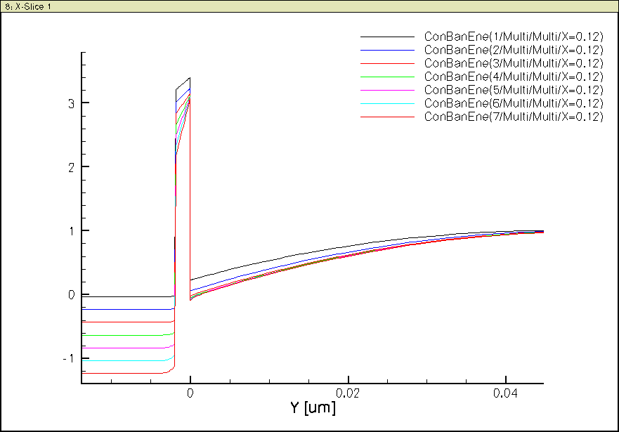
Figure 15: Band diagrams - Ec
You might better see the difference in band bending amount between the region inside the gate oxide and the region near the Si surface from the Ec plots.
Also observe that there is indeed a noticeable potential drop inside the heavily doped N+ polysilicon gate, which is responsible for the so-called poly depletion effect. That is one of the reasons why in most advanced CMOS, metal gate replaced polysilicon gate.
Just for completeness, let us look at the Ev diagrams shown figure 16: too:
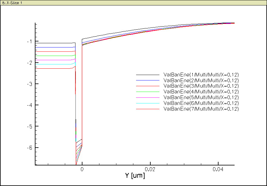
Figure 16: Band diagrams - Ev
2.7.5. Inversion Charge and Space Charge
From the band diagrams, you should have expected the following inversion carrier density distributions, in this case, n vs depth plots of figure 17:
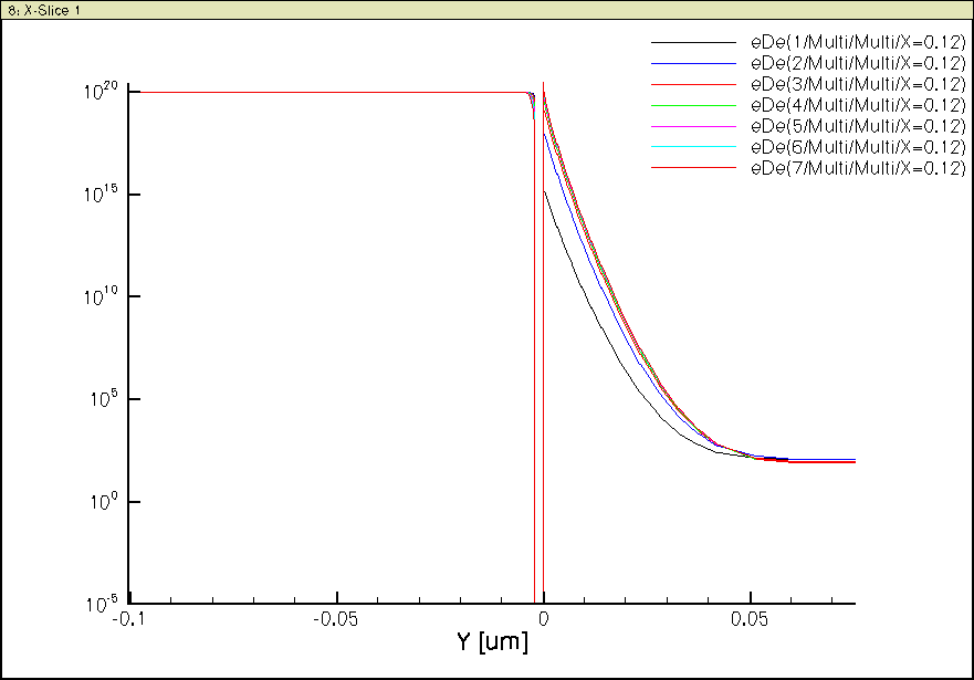
Figure 17: Electron density distribution for all gate biases
The p vs depth plots look like that shown in figure 18:
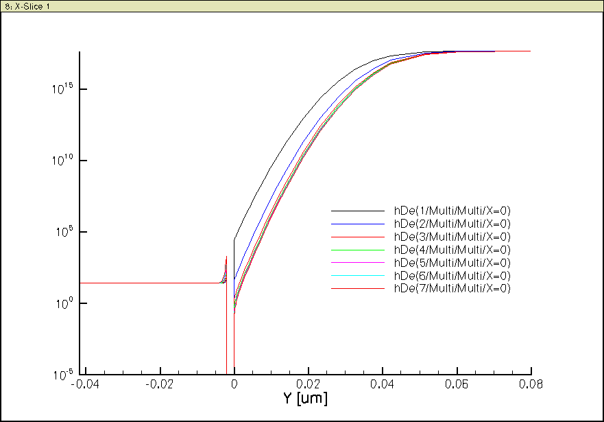
Figure 18: Hole density distribution for all gate biases
The net space charge density, defined by p-n+NdPlus-NaMinus, is shown in figure 19:
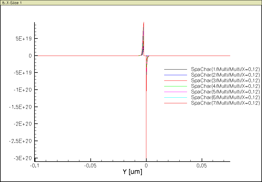
Figure 19: Space charge density distribution for all gate biases
A linear y-axis scaled is used by design here to make the point that a high spike of positive charge density exists near the gate/oxide interface. These positive charges are due to depletion of the N+ dopants in the N+ poly gate. Even with an extremely heavy 1e20 gate doping, we are still seeing quite a bit poly depletion.
As we will learn later, and some of you might intuitively expect just by inspecting the above plot, the thickness of poly depletion is comparable to the very thin gate oxide thickness. This effectively degrades the gate capacitance, as the depletion layer is in series with the gate oxide.
2.7.6. Electric Field
The e-field distribution should not be surprising. Once surface is heavily inverted, the surface e-field increases strongly, however, near the surface only, so that there is large surface e-field increase, but little surface potential increase, as shown below in figure 20:

Figure 20: Vertical electric field distribution for all gate biases
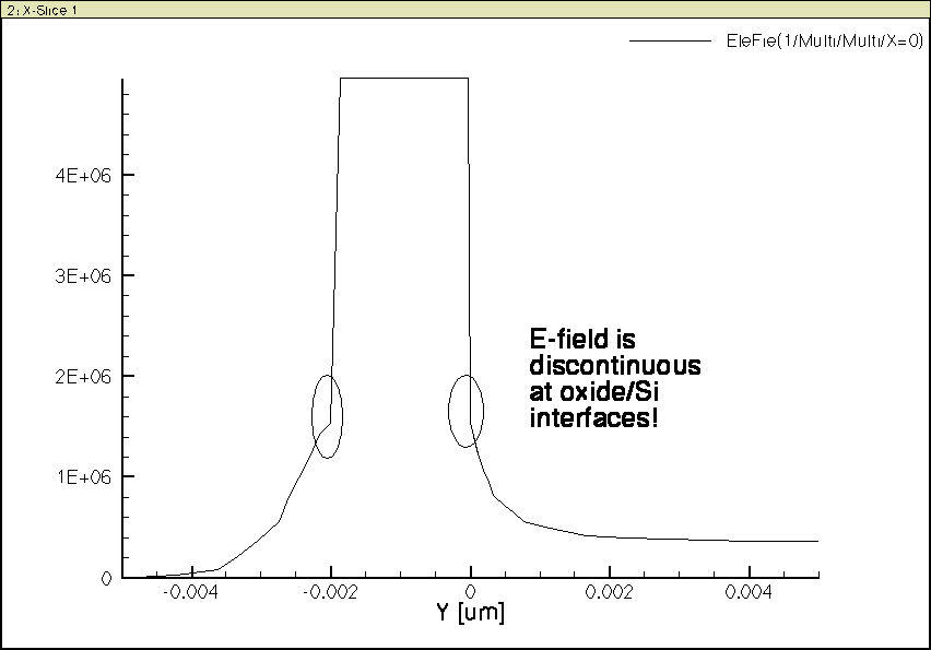
At this point, I would like to remind you of the boundary condition for electric field at the gate oxide/Si interfaces. Assuming there is no interface charge, i.e. the interface is clean and free from interface charges, fixed or variable, the normal component of electric field should be continuous across the interface.
As dielectric constant of oxide is 3.9, while that of Si is 11.7, there is approximately a 3 times difference between the oxide field and the Si surface or interface field. To show this, I have made a zoomed in plot of the electric field in the oxide and near the two interfaces in figure 21: