


Next: About this document ...
NELSON, NAGLE, CARROLL, IRWIN
DIGIAL LOGIC CIRCUIT ANALYSIS AND DESIGN
ERRATA
Last Update - 04/11/02
Asterisk * indicates errata reported after 4-1-96, when
corrections were made for the first reprint. Double asterisk **
indicates new errata reported in 2002.
- Pg. 63.
- Table 1.11. At the very top, move the subscript 4
to the left so that the column label reads
 .
.
- Pg. 93.
- Table 2.4(b). The label 11 on the 3rd row of the table
should be changed to 10, and the label 10 on the bottom row
of the table should be changed to 11.
- *Pg. 106.
- Figure 2.4, Symbol Set 2. Remove input b from the NOT
gate. This gate should have only one input, a.
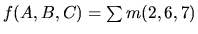
- *Pg. 170.
- Problem 2.26. Change f(A,B,C) to f(A,B,C,D).
- *Pg. 180.
- Example 3.4, 2nd line. There should be a "Sigma" symbol
in front of the minterm list:
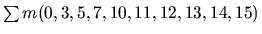 .
.
- *Pg. 182.
- 4th line from the bottom. There should be a "Sigma" symbol
in front of the minterm list:
 .
.
- *Pg. 206.
- 3rd line from the bottom, end of the line. Change
 to
to  .
.
- *Pg. 241.
- Problem 3.60, both parts (a) and (b). Change f(A,B,C,D) to
f(A,B,C,D,E).
- **Pg. 252.
- Line 11 - Change "73138" to "74138".
- Pg. 253.
- Figure 4.8 (d). The inversion bubbles (circles) should be
removed from inputs A, B, C, and G1 on the left side
of the 74LS138 logic symbol.
- Pg. 255.
- Figure 4.9 (d). The inversion bubbles (circles) should be
removed from inputs A, B, C, D on the upper left side
of the 74154 logic symbol.
- Pg. 267.
- Figure 4.21 (a) and (c). Enable input El should be
labelled EI.
- *Pg. 273.
- Remove inversion bubbles from the outputs of the
NAND gates connected to inputs E2-E15. These should be AND
gates.
- *Pg. 275.
- Figure 4.27 (d). Change "Strong" to "Strobe" at 1G-bar
enable.
- *Pg. 275.
- Figure 4.27 (e). Label "1G" and "2G" enables as active
LOW. The correct pin number for the 1Y output is 7; the 2Y output
should be labeled pin 9.
- *Pg. 276.
- Figure 4.28 (a). Label pin 4 output as "1Y" and pin 14
input as "4A."
- *Pg. 280.
- Figure 4.32 caption and Figure 4.32 (b). Change lower case
x to capital X for consistency in the example.
- Pg. 327.
- Problem 4.41. Change ``(Hint: Use the cascade inputs to
compare the two least significant digits; use one AND gate.)"
to read ``(Hint: Use the cascade inputs to compare the two most
significant digits.)"
- **Pg. 398.
- Figure 4.28(c). Remove the NOT gate at the bottom input
to the R input of the bottom NOR gate.
- *Pg. 406.
- Figure 6.22 (b). The arc from state 1 back to state 1
should be labelled ``d0" instaed of ``0d".
- *Pg. 408.
- Figure 6.25 (b). Change ``JR" to ``JK."
- Pg. 410.
- Figure 6.28(b). The flip-flop inputs are mis-labelled
on the left side of the symbol.
Change the upper input name from Q to D and the lower input
name from Q to C. Delete the '76 near the upper output.
- *Pg. 411.
- Figure 6.30 (a). Labels ``tPHL and tPLH" at the bottom
of the timing digram should be swapped.
- *Pg. 411.
- Last sentence on the page reads ``...values for both
 and
and  , from the TTL manual [1], are listed
in Figure 6.30b
as 0 ns." Change to read ``...values for and
, from the
TTL manual [1], are listed in Fig. 6.30b as 40 ns and 25 ns,
respectively."
, from the TTL manual [1], are listed
in Figure 6.30b
as 0 ns." Change to read ``...values for and
, from the
TTL manual [1], are listed in Fig. 6.30b as 40 ns and 25 ns,
respectively."
- *Pg. 412.
- First sentence reads ``...transferred to the flip-flop
output Q at the exact instant..."
Change to read ``...transferred to the flip-flop output Q at
either 40 ns or 25 ns from the exact instant..."
- *Pg. 420.
- Middle of the page - Change capacitor value from
C=
 to
to  .
.
- **Pg. 437.
- Figure 7.3(b) - under the table heading "Outputs",
the time should read
 instead of
  (the 8 is
part of the subscript).
(the 8 is
part of the subscript).
- **Pg. 439.
- End of line 11 - change "flip-flips" to "flip-flops".
- **Pg. 444.
- Figure 7.6(d). The pulse on Data line F should not
be there, since the value is "L" (low).
- **Pg. 457.
- Line 15. The subscript for the second clear line should
be 0(2) instead of O(2) (zero instead of letter O).
- *Pg. 466.
- Figure 7.19 (c). Fix three errors on the wire driven
by
 near the bottom left of the figure.
- Change the inverter driven by
to a buffer by
adding an inversion bubble to its input.
- Remove the first dot to the right on the wire driven by this inverter.
(The inverter output should not be connected to the vertical wire
driven by the AND gate below it.)
- Find the vertical wire connected to the upper three flip-flop
CLR inputs. This should also be connected to the wire driving
the bottom flip-flop CLR input, and not to the wire immediately
below it (i.e. move the vertical wire and dot
up from the feedback wire driven by the QD output.)
- **Pg. 473.
- Figure 7.23. Below the logic diagram, change (a) to (c).
Also, the lower Q output of flip-flop C in that diagram should have
an inversion bubble (Q-bar output).
- Pg. 492.
- Figure 7.36(c). In the logic diagram, at the left bottom,
the AND gate whose inputs are Strobe (10) and Clock (9)
should have inversion bubbles on both inputs.
- Pg. 498.
- Problem 7.1. The problem refers to Fig. 4.29. This
should be changed to Fig. 4.34.
- Pg. 500.
- Problem 7.15 refers to Problems 7.8, 7.10, and 7.12. These
should be Problems 7.9, 7.11 and 7.13.
- Pg. 500.
- Problem 7.16 refers to Problems 7.9, 7.11, and 7.13. These
should be Problems 7.10, 7.12 and 7.14.
- Pg. 500.
- Problem 7.16 refers to Fig. 7.34b and then to Fig. 7.34.
These should be Fig. 7.34 and Fig. 7.34c, respectively.
- **Pg. 508.
- Line 17 - Change "Fig. 8.1b" to "Fig. 8.1".
- *Pg. 532.
- Figure 8.30, in the K-map for R2, change the entry in the
top row (row 00), right column (column x=1), from ``0" to ``1".
- Pg. 623.
- Problem 9.10, 2nd line, change ``using the given state assignment"
to ``using each of the three unique state assignments", and then
delete the state assignment given next to the state table.
- Pg. 677.
- Problem 10.10, 3rd line presently reads ``If
 and
and  changes from 0 to 1..." The first subscript should be changed to
1 so as to read: ``If
changes from 0 to 1..." The first subscript should be changed to
1 so as to read: ``If  and changes from 0 to 1..."
- Pg. 680.
- Problem 10.17. The bottom row of the excitation table should
be labelled 11 and the next row up should be labelled 10,
to correspond with the circled stable states in those rows.
- Pg. 735.
- Figure P11.8. The AND gate driving flip-flop clock input C1
should be changed to a NAND gate (add an inversion bubble to
its output.)
- Pg. 737.
- Problem 11.25 change ``PDL state machine model" to ``PDL model".
- Pg. 742.
- Last paragraph reads ``A test
 for fault
  is...''.
Change the subscript on the
is...''.
Change the subscript on the  from
from  to
to  , , i.e. change
to
, , i.e. change
to  .
.
- Pg. 776.
- Figure 12.26. At the top left, the 2-to-1 multiplexer selecting
between Scan-in and the feedback signal should have a control
input connected to input line B1.
- Pg. 785.
- Figure P12.15. The OR gate input marked
 should be
connected at its left end to the vertical line corresponding
to y2, rather than to line y1.
Also, at the output of the inverter driven by flip-flop output y3
there should be a ``dot" to show a connection to the vertical
line that ends there. (The other end of the line connects to
the gate input marked
should be
connected at its left end to the vertical line corresponding
to y2, rather than to line y1.
Also, at the output of the inverter driven by flip-flop output y3
there should be a ``dot" to show a connection to the vertical
line that ends there. (The other end of the line connects to
the gate input marked  .)
.)
Next: About this document ...
Victor P. Nelson
2002-04-11