Scan-based Delay Testing
Delay testing is becoming important to guarantee the quality of the IC chips. Many defects in deep sub-micron (DSM) designs will assume some small extra delay that only impact the signal paths within 20~50% of the critical path delay of the circuit, which can be missed in traditional stuck-at test. Intel shows that typical delay defects will cause around 500DPM for a particular design without delay test. Note that commercial DPM requirement is around 100DPM. Thus delay test has attracted more research effort recently.
The delay test can only be employed based on some pre-exist faulty models. There are several different delay fault models, including gate delay model, segment delay model, transition delay model and path delay model. Among all of them, transition delay model and path delay model are the most popular two models.
Transition delay model assumes that the delay defect will cause a gross delay effect in one gate. To test delay fault, the <V1, V2> pair needs to activate the transition through that gate. The output is thus observed and if an error is found, then the delay defect is detected. Note that the fault space (total number of fault under test) is two times of the gate number in the circuit. (For each gate, we need to test both rising and falling transitions.) This model is simple to use and the fault space is small. The disadvantage is that it can miss the delay faults that are caused due to distributed delay defects, which impact multiple gates at the same time.
Path delay model comes to solve this deficiency incurred by using gate delay model. Basically all the signal paths in a design are tested by properly choosing <V1, V2> test pairs. Ideally if a circuit passes a path delay test, it can be 100% free of delay defect. But the difficulty for path delay test is that the number of the fault space is too large. In worst cases, the size of the fault space is an exponential function of the number of the gates in circuit.
The current industry practice for delay test is the combination of both delay tests mentioned above. First 100% (or nearly 100%) transition delay test is performed. If the chip passes the transition delay test, then some of the critical paths are selected to perform path delay test.
Scan-based delay test poses other difficulty that is in scan chain, the applicable <V1, V2> pairs are restricted due to the structural limitation of the scan chain. Some other scan design techniques can be used to store two bits at the same time, which is called enhanced scan chain design. But it is not an appealing solution due to its large impact on circuit performance. Thus we are only considering the delay test in standard scan based design.
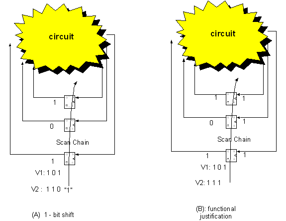
Basically there are two types of techniques that can be employed in scan-based delay test. One is called 1-bit shift (IBM calls it “skewed load”), where V2 is one bit shift of V1. The other is called functional justification (IBM calls it “broadside”), where V2 is the functional responses of the circuit with the application of V1. Figure 1 shows two cases.
In large designs, 1-bit shift scheme doesn’t work well due to its strict requirement for controlling the clock signals. And functional justification is used in most scan-based designs.
We are focusing on 1-bit shift scheme, which is doable in small designs. We can also try to test the chips using functional justification test set after the chips come back.
The way to determine how to choose where to insert our delay elements and how to generate the corresponding test vectors are shown in the following.
1) Initialized the scan chain by scanning vector. For example, all “0” vector. Choose to monitor the inputs to scan cells by tracing the waveforms in those lines.
2) Applying random <V1, V2> pair at primary inputs (PI), and scan in one bit “1” or “0” depends on your preference.
3) If there is transition observed in the inputs to the scan cells, then trace back about 2 ~ 3 logic levels away from the inputs, the corresponding lines are the candidate spots to insert delay elements.
4) The transition can be activated by PI only or from the application of the outputs from scan chain. In order to only activate the transition by scan chain, you can fix the <V1, V2> pair. For example, apply the same two vectors to PI, observe whether there is any transition in the input line to scan cell. On the contrary if the transition is required to be activated from PI only, then you can scan in all “0”/”1” and make the V1, V2 pair within scan chain the same.
5) The minimum requirement in this experimental study is that the delay effect has to be captured by scan cell. Which requires that the delay effect be sensitized to scan chain.
In order to allow maximum freedom and try as many different approaches as possible, we want the designs be accomplished independently. Apart from this, the basic requirement as shown above has to be implemented.