PTAT Simulation Example
Using PSPICE 9.1
Let’s simulate a PTAT (Proportional to Absolute Temperature) circuit and analyze its performance over temperature.
Note: If you will be working on more than one machine, refer to the appendix: Changing Simulation Directories and Avoiding Library File Errors.
1. DRAWING THE SCHEMATIC
Start PSPICE Schematics on your machine by double-clicking this icon or selecting it from the Start menu:
![]()
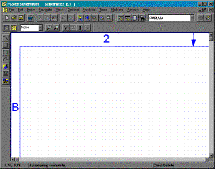
Schematics should open with a blank drawing page that looks something like this:
Make sure the grid is on by selecting Options/Display Options and checking Grid On and Stay-On-Grid.
Save your new blank schematic into a new folder. It is important to put each schematic you work on into a separate folder, since a number of files are generated during simulation that must be kept together.
We will begin by placing all the required parts on the schematic. Refer to the screen shot several figures below to see the final parts layout.
First we will place two PNP transistors. Use CTRL-G to bring up the Get New Part dialog box:
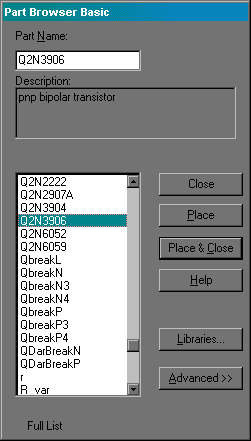
Type Q in the Part Name field, select the Q2N3906 part, then press Place & Close.
The cursor will drag around the part. Place it somewhere on the page by left-clicking the mouse. Place a second copy nearby by left-clicking again. Then let go of the part by right-clicking.
Orient and position the parts. Click on a part to highlight it red. Then you can drag it with the mouse, rotate it using CTRL-R, and flip it using CTRL-F.
Note: You can zoom in and out using the toolbar buttons:
and you can use the window sliders to navigate around the page. Sometimes during editing spurious marks will be left on the page. You can clean up the drawing anytime by selecting View/Redraw or CTRL-L.
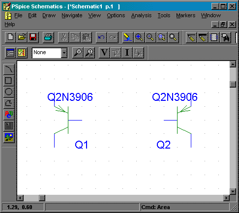
Your page should look similar to this:
Now change the part names to Q3 and Q4. Double-click on the “Q1” text block and change it to Q3. Likewise change “Q2” to Q4. Also, you can single-click on any text block and drag it to a more suitable position.
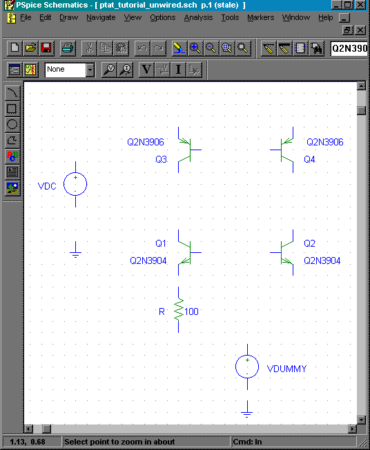
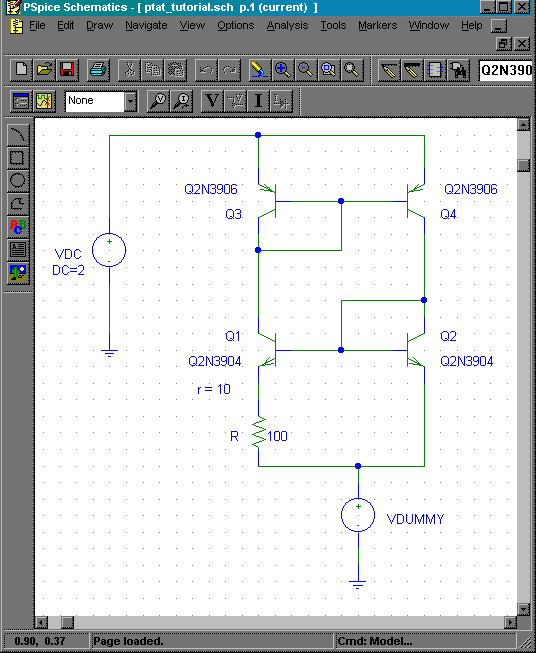
Next, place two Q2N3904 NPN BJT’s on the schematic. Label them Q1 and Q2. Also place two VSRC voltage source parts. Label one VDC and the other VDUMMY. Place one resistor (R) and label it R. Double-click the value text block (default is 1k) and change it to 100. Finally, place two copies of EGND (earth ground). After placing, naming, and arranging the parts, your drawing should now look similar to this:
Note: You can move a collection of items simultaneously by first dragging a selection box around them, and then moving the selection. To create a selection box, left click the mouse button and drag across the desired region. When you let go of the mouse button, all selected items will turn red.
Next, wire the parts. Use CTRL-W to activate the wiring tool. The cursor will turn into a pencil. Move the cursor to the desired starting point of a wire, then left-click and release to start the wire. Move the cursor toward the wire’s destination. A dashed line will follow the cursor. You can go in a straight line, or make one 90o turn just by moving the mouse. In order to make a second 90o turn, left click the mouse, then move in the desired direction. When the wire reaches its destination, left-click to fix the wire end. The wiring tool will remain active so you can begin a new wire. To disable the wiring tool and return to the regular cursor, right-click the mouse. To delete a segment of wire, select it and press the delete key. Wire the parts as shown below (the connection dots appear automatically whenever more than two wires meet):
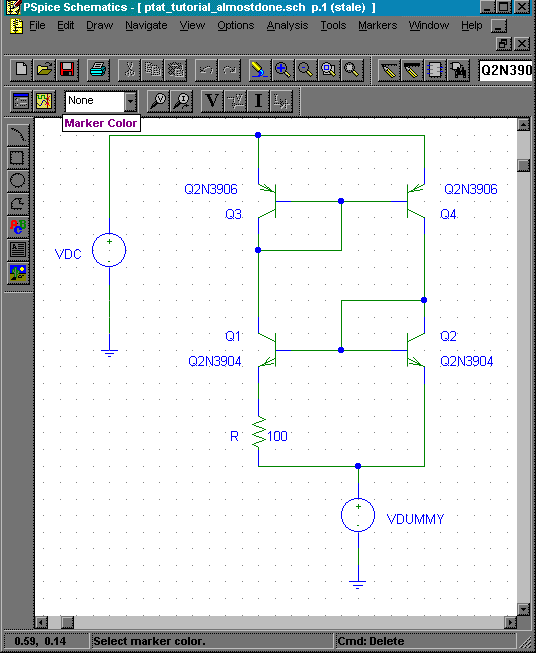
The schematic is now complete. Be sure to save it (use File/Save, CTRL-S, or the disk icon on the toolbar).
The next step is to assign a value of 2V to VDC. Double-click on the VDC part to bring up its parameter box:
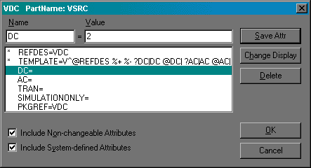
Select the DC= line. In the Value box, type 2. Click the Save Attr (save attribute) button. Click the Change Display button to bring up the Change Attribute box:
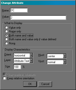
Check the radio button under “What to Display” labeled Both name and value. Click OK, then OK to return to the schematic. The text DC=2 should appear near the VDC part. Drag it to a suitable location.
The next step is to modify the area of Q1 and setup the simulation.
We want to set the area ratio of Q1 to Q2 to be r = 10. We will do this by modifying the saturation current parameter of Q1. Select Q1 by clicking on it. It should turn red. Then from the main menu select Edit/Model. The following dialog box should appear:
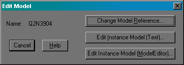
Click on the Edit Instance Model (Text) button. You should get the following parameter editing box (Notice that the model name on the first line has changed to Q2N3904-X. This indicates that the model has been modified from the built-in Q2N3904 model.):
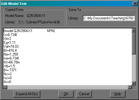
We want to change the Is parameter (saturation current) from its current value of 6.734f (that’s 6.734E-15) to 10 times that value. Edit the value to 67.34f and click OK to save it. There will be no indication of this change on the schematic. In order to remind yourself of the change, you can add a text box. Use Draw/Text or Draw/TextBox to place text anywhere on the drawing. Place a text box with “r = 10” near Q1. Clean up any spurious marks using CTRL-L (View/Redraw).
The schematic should now look similar to this:
2. SETTING UP THE SIMULATION
Now you are ready to setup the simulation. Select Analysis/Setup or click the Setup icon

to get the following dialog box:
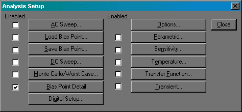
Note that Bias Point Detail is checked by default. This will solve for all DC currents and voltages at the specified temperature. PSPICE uses a temperature of 27 oC by default. For our analysis, we need to vary the temperature and examine the current through VDUMMY. Click the Temperature button, change the temperature to –100, click OK, the Close the Analysis Setup box.
3. RUNNING THE SIMULATION
Run the simulation by choosing Analysis/Simulate or pressing F11. You can also click the icon:

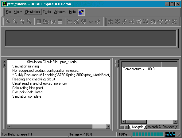
This will start the PSPICE simulator. It will check for errors and then try to run the simulation. What you see next depends somewhat on the configuration of the installation you are using, and whether there are any errors in your schematic. If there are no errors, you should get a window that contains a report similar to the following:
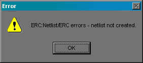
If the circuit has errors, you may get an error box like this one:
When you click OK, you might get a detailed report like this:
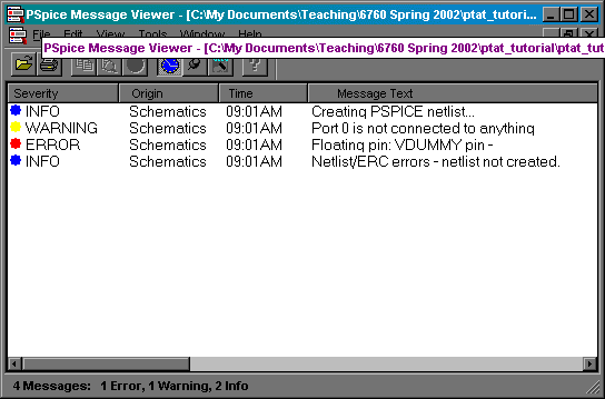
Careful reading of the error messages can usually help pinpoint the problem. In this case, the wire connecting VDUMMY to ground was left out. Close the error box, fix the schematic, and run the simulation again.
Another common type of error involves missing Library files. This usually occurs after trying to copy the simulation from one machine or folder to another. A more complete discussion of this is included in the Appendix – Changing Simulation Directories and Avoiding Library File Errors.
4. GETTING THE RESULTS
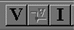
If the simulation runs successfully, you can close the simulation window and return to the schematic window. Clicking on the Display Voltage or Display Current icons will show the values on the schematic.
These are toggle buttons. To turn off the display, click them again.
After simulating at –100 oC and displaying current, the schematic window should look like this:
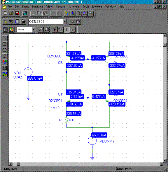
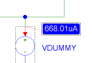
The text boxes containing current values can be dragged using the mouse. When a box is selected, a red arrow will appear indicating the branch and direction of the referenced current, as shown in the close-up of the PTAT current below:
You should manually record the value of current, and then continue analyzing the PTAT at various temperatures. To continue, return to the setup dialog box, change the temperature, and run the simulation again. Any displayed currents and/or voltages will be updated automatically.
Although the method described here requires you to simulate and record the results at each temperature (e.g., on a spreadsheet), it is possible to cause PSPICE to perform an analysis over temperature automatically using Parametric Analysis (Analysis/Setup/Parametric). This will be covered in a later tutorial.
Appendix – Changing
Simulation Directories and Avoiding Library File Errors
PSPICE keeps track of device parameters (for BJT’s, for example) in separate files called library files (*.lib). These files are required in order for the simulation to run. Most library file errors occur when a user copies a simulation from one folder or machine to another, and fails to keep the accompanying library file(s) intact with the Schematics (.sch) file. The built-in library files contain the factory list of parts supplied with PSPICE, and are usually not a problem since each installation of PSPICE contains them by default. However, if you modify a library part or create a blank part from scratch (breakout part), Schematics will create new library file(s). The library files being used in a current schematic can be viewed and manipulated by choosing Analysis/Library and Include Files. Here is an example from the PTAT simulation:
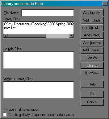
This box shows two library files in use. The first,
C:\My Documents\Teaching\6760 Spring 2002\ptat_tutorial\ptat_tutorial.lib
(In Schematics, the full path and filename could be
viewed by using the slider.)
is a reference to a local library file created in the same directory as the .sch file. (This was created when we modified the Q2N3904 model to increase the Is parameter.)
The second, nom.lib*, contains the factory definitions of all parts supplied with this installation. The trailing asterisk indicates that this is to be available to all schematics. This file is located somewhere in the PSPICE installation directory structure on each machine.
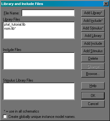
In order to move the simulation from one folder or machine to another, it is necessary to copy both the .sch file and any local .lib files. However, since the reference to the local library file includes a complete path name, Schematics will try to follow that path in the new destination, and report a “missing library file error.” The easiest fix for this is to edit the local library file reference to remove the path name. Then Schematics will always look in its current directory, and you can copy it anywhere as long as you keep the .sch and .lib files together.
To edit the library file reference, click on its name in the list, and it will appear in the File Name box at the top. Edit out the path name, leaving just the file name. Click the Change button. Confirm that the edited library file name appears in the list:
Then click OK to return to the schematic.
You should now be able to move your simulation by copying the .sch and .lib files together.
A more comprehensive method for moving large simulations and their associated results files is provided through PSPICE Design Manager, which automatically opens whenever Schematics starts. Design manager refers to a simulation folder as a Workspace, and provides a menu for moving Workspaces from one location to another. It automatically modifies internal references and updates paths as needed.